


Why Apple Manufactures in China (And What Hardware Startups Can Learn From Its Playbook)
When asked why Apple manufactures in China, ‘cheap labor’ is the facile answer. The more accurate one is supply chain engineering. A modern iPhone may
 5 Star Rating on
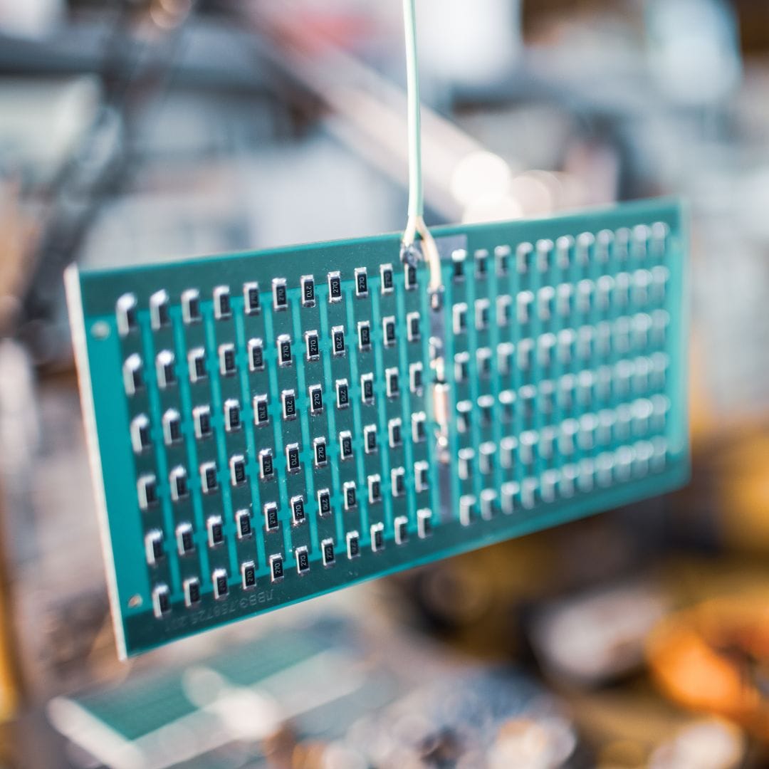
 Package on Package (PoP) assembly is a method of stacking integrated circuits. It combines separate logic and memory packages into one unit. This technique saves space and boosts performance in electronic devices. OurPCB offers expert PoP assembly services for your advanced packaging needs.


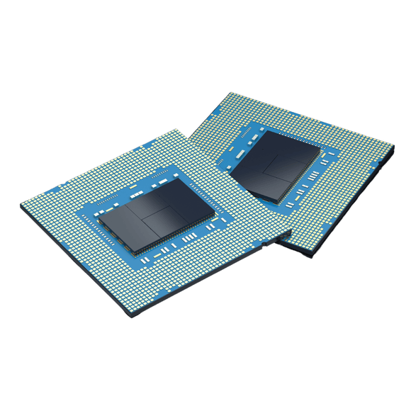

PoP assembly stacks two or more IC packages on top of each other. The bottom package often contains logic chips, while the top holds memory components. This setup allows for direct vertical connections between the packages.
The assembly process precisely aligns and solders the packages. Solder balls on the bottom of the top package connect to pads on the bottom package. This creates a compact, high-performance module ideal for space-constrained applications.


OurPCB brings expertise, quality, and efficiency to your projects with our PoP assembly services. Our advanced capabilities ensure optimal results for your semiconductor needs.


PoP technology offers significant advantages for modern electronics. It combines high performance with space efficiency, making it ideal for compact devices.


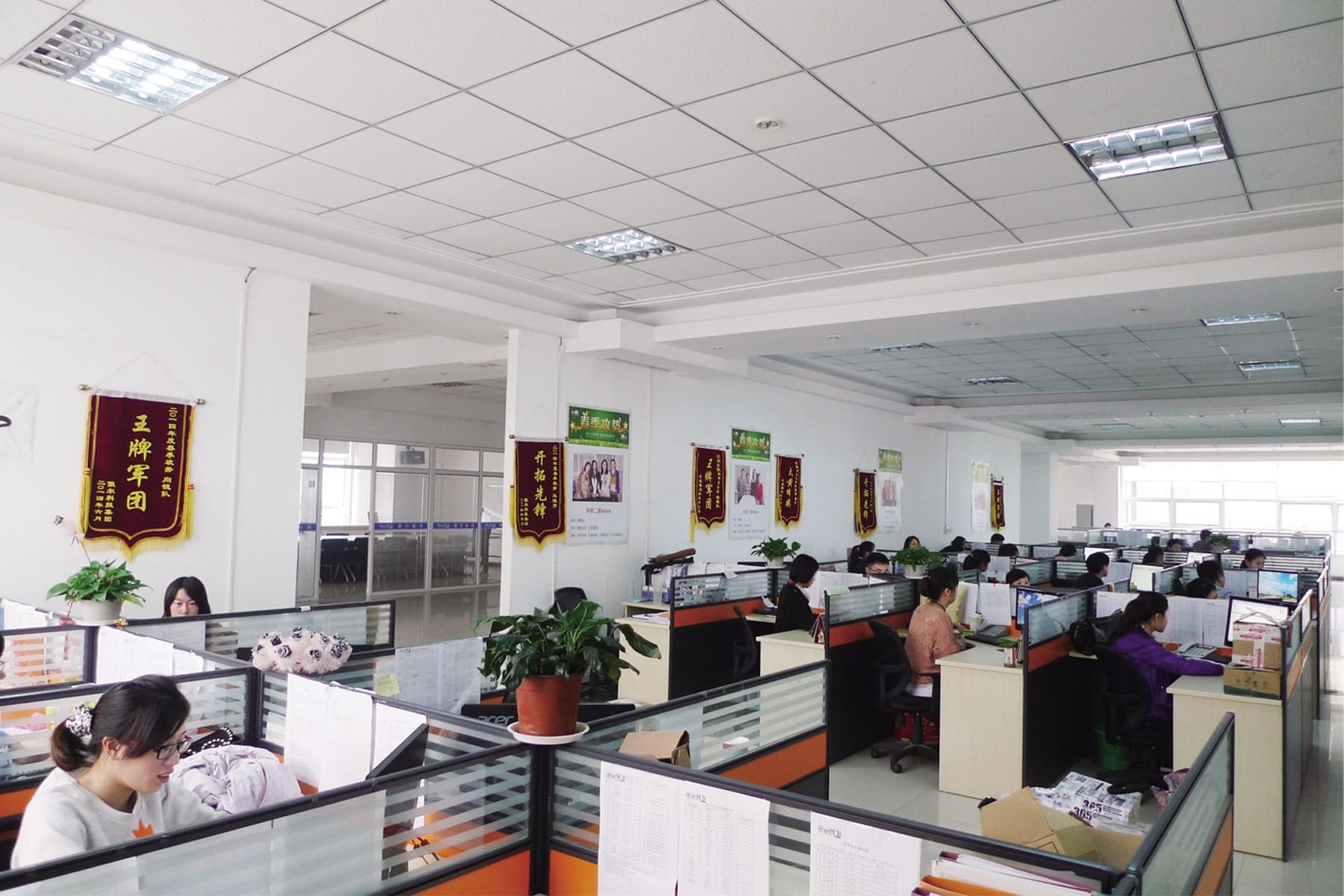
OurPCB offers a wide range of PCB assembly services to meet diverse needs. We combine precision, quality, and efficiency in every project.

We use advanced Surface Mount Technology for high-density, compact PCB assemblies. Our SMT process ensures precise component placement and reliable connections.

We adapt to your needs, working with your supplied components or providing full turnkey solutions. Our services cover everything from sourcing to final assembly.

Our team creates tailored PCB assemblies to match your exact specifications. We handle unique designs and special requirements with skill and attention to detail.

We offer fast, high-quality PCB assembly services. Our efficient processes deliver quick turnarounds without compromising on quality or reliability.

We produce PCB assemblies that meet strict IPC Class 3 standards. This ensures top performance in critical applications like aerospace and medical devices.

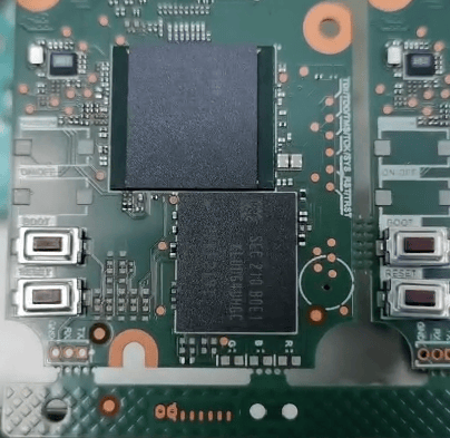
We handle a wide range of IC package types in our PCB assemblies. This includes BGAs, POPs, CGAs, QFNs, DFNs, and CSPs, all assembled with precision.
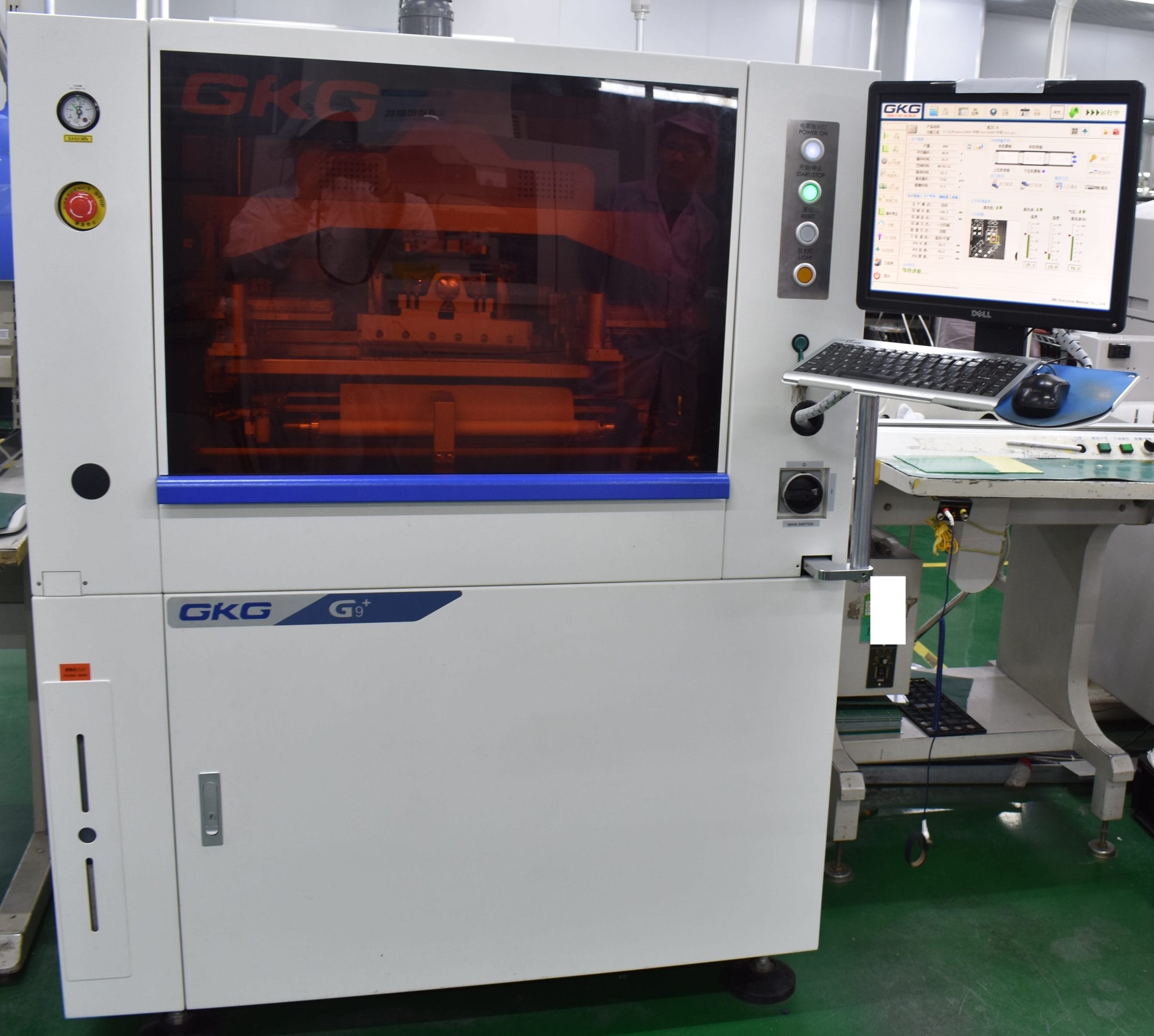
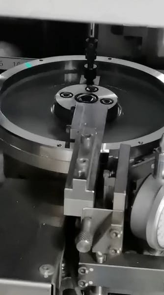
OurPCB possesses advanced technical capabilities for PoP assembly. We handle complex package stacks with precision. Our equipment allows for fine-pitch connections down to 0.25mm. We use X-ray inspection to ensure perfect alignment and solder joint quality. Our thermal management techniques optimize heat dissipation in dense package stacks.
Mon-Fri: 24 hours,
Sat: 9am-6pm, GMT+8
Reach us at
[email protected]
24 hours online
+86-199-30589219
Mon-Fri: 24 hours
Sat: 9am-6pm, GMT+8
The package-on-package assembly process stacks package components like a logic package and a memory chip for higher density. The PoP process involves placing the bottom PoP on the substrate, applying solder paste, and aligning the upper package. Ball grid array (BGA) connections ensure interconnection between the top and bottom packages through reflow soldering. A typical logic plus memory PoP stack improves electrical performance and integrates processor and memory efficiently.
The PoP manufacturing process faces more thermal challenges due to its 3D package design and higher component density. PoP provides better heat dissipation strategies by optimizing integrated circuit packaging and improving airflow. PoP allows efficient heat removal by adjusting system in package configurations and using materials like those from Indium Corporation. Unlike package in package, thermal solutions in semiconductor manufacturing must address heat transfer from the bottom of the package upwards.
Warpage in PoP uses results from mismatched thermal expansion between the lower package and the upper package. Uneven reflow soldering and variations in flash memory or discrete logic and memory contribute to deformation. Techniques from advanced semiconductor engineering control warpage by adjusting baseband materials and PoP manufacturing process conditions. Moreover, maintaining even heating during assembly prevents excessive warping in embedded PoP structures.
The SMT PoP process assembles PoP uses through surface-mount technology, stacking components for higher component density. BGA and ball grid array ensure strong interconnection between the top and bottom layers. Semiconductor manufacturing advancements optimize PoP process efficiency in high-performance applications. This method enables flexible processor and memory configurations with improved advantages of PoP in miniaturized electronics.
When asked why Apple manufactures in China, ‘cheap labor’ is the facile answer. The more accurate one is supply chain engineering. A modern iPhone may

PCB tariffs from China can significantly change the real cost of a U.S.-bound order before your boards reach production. A quote may look competitive at

Wire harness tariffs from China commonly fall under HTS 8544.30, the U.S. Harmonized Tariff Schedule (HTSUS) classification for ignition and other wiring sets used in

Unverified wire harness suppliers pose significant risks that often surface long after delivery. A weak crimp, wrong insulation material, missing UL rating, or undocumented connector

Placing an initial Purchase Order (PO) with an unverified China-based PCB supplier can critically jeopardize your budget, launch timeline, and product quality. Knowing how to
Underwriters Laboratories (UL) help engineers, buyers, and manufacturers choose wire and cable that can safely perform in specific electrical, mechanical, and environmental settings. These standards
We use cookies to improve your browsing experience, which may include personal information. By clicking "Agree," you accept our Privacy Policy and cookie use. You can change your cookie settings in your browser anytime.
Agree Chat With Us
  Free Quote