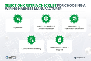
Top 10 Classic Car Wiring Harness Manufacturers | Full Guide
Finding the right wiring harness manufacturer for your vintage ride can be a real headache. Those beautiful old machines need special wiring that looks period-correct

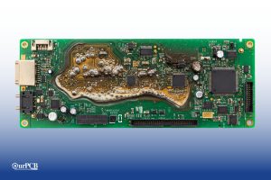
OurPCB provides production-grade PCB soldering services for circuit board assemblies requiring controlled thermal profiles, high-yield wetting, and Class 2/3 solder joint conformance across SMT, through-hole, and BGA/QFN packages.
We control every soldering variable: tip temperature, dwell time, solder alloy type, flux activation window, and nozzle position to eliminate bridging, cold joints, and voiding during high-density assembly.r.


At OurPCB, PCB soldering is fully integrated into our in-house PCB assembly process, forming the link between automated component placement and multi-stage inspection.
We apply thermal bonding methods that meet the mechanical, electrical, and environmental demands of modern assemblies, including SMT, through-hole, and hybrid designs. Our soldering workflows are sequenced for zero-process disruption and Class 2 or Class 3 yield compliance.

Once components are placed on the printed circuit board using high-speed pick-and-place machines, each board moves directly into its assigned soldering process. For SMT assemblies, we apply solder paste using stainless steel stencils aligned to pad geometry, followed by optical registration checks.
For through-hole components, we use a dual-wave line with top-side preheating to 266 °F (130 °C), flux activation, and immersion in molten solder at 482 °F (250 °C) with conveyor speeds between 1.2 and 1.8 meters per minute. Every soldering path is selected based on component type, thermal sensitivity, and board design constraints provided by the customer.
We synchronize all soldering techniques with the board’s construction, copper weight, and material limitations. In mixed-technology assemblies, we apply selective soldering when reflowed SMT components require thermal isolation during through-hole soldering.
Our selective soldering machine uses a programmable nozzle path and radiant preheating to 212 °F (100 °C) to avoid heat-related warpage, pad delamination, or microcracking. Every thermal profile matches the board’s stackup, copper distribution, and IPC tolerances to maintain proper wetting and protect against stress-induced defects.
Soldering is followed immediately by downstream inspection using automated optical inspection, 3D X-ray, and in-circuit test. This placement–solder–inspection chain is tightly controlled by OurPCB’s MES and ESD process systems.
It enables traceability across every circuit board and ensures defect capture before final test or shipment. Any joint failing Class 2 or Class 3 criteria is automatically queued for manual soldering, rework, or engineering review.
OurPCB is a PCB soldering service manufacturer certified to the highest global standards for assembly reliability and quality control. We support prototype and volume builds with thermal accuracy, process traceability, and Class 2 or Class 3 solder joint conformance on every board.

We are certified to IPC-A-610 Class 2 and Class 3 workmanship standards, covering all solder joints, terminal connections, and component mounting across our SMT, THT, and mixed-technology lines.
All internal process controls follow ISO 9001:2015 and IATF 16949 protocols for electronics manufacturing.
This framework governs our full PCB assembly and soldering services, including document control, first-article validation, and inspection escalation procedures.

We operate dual Fuji pick-and-place machines for high-speed placement accuracy down to ±50 microns, supported by precision stencil printers and nitrogen reflow ovens with controlled peak temperatures of 464 °F (240 °C) for lead-free profiles.
Our wave soldering systems offer dual-wave capability for through-hole components at immersion temperatures up to 482 °F (250 °C).
For inspection, we deploy 3D X-ray, automated optical inspection, in-circuit testers, and 3D SPI for solder paste volume analysis.

As a proven PCB soldering service exporter, OurPCB supplies full board assemblies to OEMs and contract manufacturers across North America, Europe, and Southeast Asia.
We manage export documentation, packaging protocols, and international shipment tracking for turnkey projects.
Our production systems support volume PCB assembly, RoHS compliance, and full traceability for customer-supplied or sourced BOMs.

Our production team manages complex assemblies involving mixed SMT and Through-hole components, specialty connectors, and unique board configurations.
We coordinate procurement, soldering, and test workflows for turnkey builds and multi-stage delivery cycles, ensuring on-time output for prototype and high-mix orders.

We conduct detailed manufacturing reviews of customer-supplied Gerber files, BOMs, and assembly drawings to identify risks before production.
Our team evaluates pad layout, solder mask clearance, and thermal relief features to match soldering requirements with actual board design constraints.
This review process supports defect prevention and high solder joint yield in every order.


We use vapor degreasing to clean fine-pitch SMT assemblies where low standoff heights prevent rinsing under components. The process heats a fluorinated cleaning fluid such as HFE-72DA until it vaporizes at 58 °C.
Our sealed-chamber systems recover 90% of solvent through closed-loop distillation and vapor filtration. Because no water is used, this PCBA cleaning method prevents capillary trapping and delivers dry, spot-free boards that are immediately ready for conformal coating or inspection.
For high-throughput cleaning, we operate fully enclosed aqueous cleaning systems that combine high-pressure spray with saponified deionized water at 60 °C. These systems target assemblies with solder paste, rosin, or water-soluble flux, removing active ions and organic residue from both sides of the board.
Our InJet platforms use 2.0 bar rotary spray heads for impingement and cascade rinsing with resistivity sensors that maintain <1.56 µg/cm² NaCl equivalent. Each cleaned board is force-dried at 70 °C for 10 minutes to eliminate moisture and prepare the surface for optical inspection or downstream processing. This is the most efficient method for batch-based PCBA cleaning at scale.
When boards require post-assembly rework or selective soldering, we apply a controlled manual cleaning process to treat localized contamination. Technicians begin by applying Decotron T383 or high-purity IPA to the assembly surface, then scrubbing with anti-static brushes at a 45° angle and 250 g pressure.
Flux is then removed using a directional aerosol rinse, and drying is completed with 30 psi filtered air or lint-free polyester wipes. This method allows us to clean the PCBA without subjecting sensitive components to immersion or thermal stress. We document all manual cleaning steps for traceability on high-reliability builds in automotive, medical, and aerospace programs.
At OurPCB, we remove no-clean flux during the PCBA cleaning process to prevent insulation resistance loss, support coating adhesion, and avoid inspection rejection in Class 2 and 3 assemblies.
Although low-solid no-clean flux is engineered to remain on the board, its residue absorbs moisture, lowers surface resistivity, and disrupts conformal coating uniformity, especially near component edges or mask-defined pads.
Our PCBA cleaning procedures are based on flux type, component density, and coating thickness requirements, and are qualified using ionic cleanliness testing, white residue detection, and surface preparation metrics that ensure coating and inspection compliance.
We remove no-clean flux residue because its remaining solids form hygroscopic films with ionic content capable of enabling leakage currents under bias. These residues often contain halide activators or rosin derivatives that, in humid environments, allow ionic mobility as low as 10⁸ Ω insulation resistance across narrow conductor spacing.
On high-density printed circuit board assemblies, especially those with ≤0.3 mm pitch, this can lead to dendritic growth, moisture-induced tracking, and eventual open or short failures. In Class 3 applications, even visually benign residues violate IPC J-STD-001 Section 8.3.1, prohibiting any visible residue under conformal coating.
Removing these residues is required to maintain dielectric performance and prevent latent field degradation.
Our cleaning strategy depends on the flux chemistry and board design. For fully assembled SMT boards, we use vapor degreasing with HFE-72DA or Vertrel XF, which condense at 55 °C – 65 °C onto the PCBA surface, dissolve polar and non-polar residues, and evaporate without leaving water or exposing components to immersion.
In rework areas or where selective cleaning is required, we use Decotron T383 or high-purity IPA with aerosol precision nozzles to rinse solder ball traps and low-solids residue from around pads.
The process is followed by 30 psi filtered air drying or vacuum-assisted drying to prevent water adsorption beneath packages. Surface prep is validated using surface insulation resistance (SIR) measurements, ionic testing (<1.56 µg/cm² NaCl equivalent), and UV light to detect fluorescence from missed residues.
Removing flux residue allows for consistent conformal coating flow and edge adhesion, especially in boards using urethane or acrylic coatings. Cleaned surfaces increase surface energy, improving film wetting and eliminating common defects like dewetting, bridging, or edge lift.
Coating adhesion strength improves from 1.2 N/mm (on flux-contaminated surfaces) to over 2.5 N/mm on properly cleaned copper and solder mask regions, reducing delamination risk during thermal cycling. In addition, a clean PCB surface ensures that automated optical inspection (AOI), UV inspection, or manual visual checks can accurately detect voids, bubbles, or skipped areas.
For applications in automotive ECUs, implantable medical devices, or high-speed digital RF systems, surface cleanliness before coating directly correlates to long-term device reliability in harsh conditions.
Our reflow lines support high-density SMT components using nitrogen convection ovens with 4-zone profiles: preheat at 320 °F to 356 °F, soak to 392 °F, peak at 464 °F ±3.5 °F, and controlled cooling. We apply lead-free solder alloys such as SAC305 using precision stencil printers and stainless steel stencils matched to pad geometry.
Solder paste volume is verified with 3D SPI before thermal processing, and final joints are inspected to IPC-A-610 Class 2 and Class 3 standards. This reflow soldering method ensures consistent wetting on all surface mount technology assemblies without warpage or oxidation.
Our wave soldering systems use dual-wave technology with fluxing, preheating to 266 °F (130 °C), and solder pot immersion at 482 °F (250 °C). Boards move through at controlled speeds between 1.2 and 1.8 meters per minute to maintain optimal dwell time.
We support through-hole technology and mixed assemblies where SMT components are shielded or pre-soldered.
This process delivers full wetting on pin and pad interfaces, preventing bridging and cold joints on high-pin-count through-hole components. Final joints are inspected per IPC-A-610 Class 2 or Class 3 acceptability standards.
We use selective soldering machines with programmable nozzle control, flux spray heads, and radiant preheat to 212 °F (100 °C) for localized soldering without thermal damage to nearby components. This method is ideal when SMT components already reflowed must be protected during through-hole soldering.
We apply this technique for shielded connectors, plated enclosures, and mixed-material builds. The system maintains ±0.3 mm nozzle precision and controlled dwell to form clean joints on isolated surface mount pads or fine-pitch terminals.
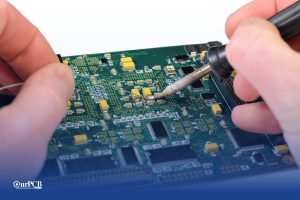
Our manual soldering operations support rework and touch-up tasks for fine-pitch leads, connector repair, and component-level updates. Operators use temperature-controlled soldering irons set between 662 °F and 716 °F (350 °C to 380 °C) with optical magnification for joint inspection and alignment.
We perform QFN rework, lifted pad repair, pin replacement, and cleanup of thermal shock failures. Minimum pad-to-pad spacing and part-to-hole spacing are validated at 50 to 100 mils. All manual work is performed to IPC-A-610 Class 3 acceptance criteria using validated repair services procedures.
Every board is inspected and tested after soldering using automated optical inspection, 3D X-ray, in-circuit testing, and microsection analysis. We classify assemblies to IPC-A-610 Class 1, 2, or 3 based on product requirements, with visual inspection focused on solder joint geometry, component alignment, and lead integrity.
For Class 3 builds, we evaluate cleanliness, mechanical stability, and conformal coating thickness between 25 and 250 microns. These combined methods ensure delivery of a fully verified, production-grade quality PCB that meets critical function and durability standards.
We support lead-free and SnPb solder systems, with SAC305, SN100C, and Sn63Pb37 alloys selected based on thermal profile, joint strength, and application environment.
Melting points range from 361 °F to 455 °F (183 °C to 235 °C), with matched flux chemistries to reduce oxidation and improve wetting on varied pad finishes. We calibrate stencil thickness from 0.10 mm to 0.18 mm, depending on component density, and apply aperture design rules to prevent bridging and slumping.
All assemblies are cleaned using solvent-safe methods to remove ionic residues and prevent dendritic growth. We evaluate solder mask quality, PCB pad surface finishes, and board layout during DFM review to confirm compatibility with our soldering systems and material limits for each printed circuit build.
Soldering defects increase the risk of electrical failure, mechanical instability, and rework costs across production.
At OurPCB, we prevent these issues by precisely controlling every soldering process parameter, from solder paste application to reflow profile calibration. Our approach combines defect detection, statistical inspection, and corrective process tuning to eliminate failure points before the final test.
| Defect | Cause | Detection Method | Our Process Controls |
|---|---|---|---|
| Bridging | Excess paste, incorrect stencil aperture, and poor alignment. | AOI, continuity test. | Optimized stencil design, calibrated paste volume, and accurate placement. |
| Solder Balling | Volatile flux, rapid heating, contaminated paste. | 3D X-ray, AOI. | Controlled ramp rate, validated solder paste handling, and nitrogen soldering process. |
| Cold Joints | Insufficient heat, poor wetting, and oxidation. | Visual inspection, continuity test. | Reflow profile tuning, molten solder temp calibration, material compatibility checks. |
| Lifted Pads | Thermal shock, excessive rework, and laminate delamination. | AOI, microsection analysis. | Ramp rate control, preheat cycles, and substrate review during circuit board rework. |
| Component Shift | Conveyor vibration, paste slump, and nozzle misalignment. | AOI, visual confirmation. | Placement vision systems, mechanical support, and short stencil-to-placement dwell time. |
Mon-Fri: 24 hours,
Sat: 9am-6pm, GMT+8
Reach us at
[email protected]
24 hours online
+86-199-30589219
Mon-Fri: 24 hours,
Sat: 9am-6pm, GMT+8
A PCB and soldering service joins electronic components to a printed circuit board by forming reliable electrical and mechanical connections at each pad location. This can involve automated SMT lines, wave soldering systems, or manual rework using temperature-controlled irons and magnified inspection.
At OurPCB, every assembly service includes matched thermal profiles, component validation, and IPC-A-610 Class 2 or 3 compliance to ensure long-term joint integrity.
Reflow soldering is used for surface mount assemblies, heating the board through a defined thermal profile to melt solder paste under SMT components. Wave soldering is applied to through-hole assemblies by passing the board over a molten solder wave, which is ideal for high-pin-count headers and sockets.
Selective soldering targets only specific joints using a programmable nozzle, avoiding thermal stress on nearby parts. Each soldering process is selected based on board layout, component density, and reflow compatibility.
OurPCB performs BGA rework and QFN rework using high-magnification inspection, thermal profiling, and 3D X-ray for alignment verification. Failed BGA packages are removed and replaced using hot gas or IR reflow, followed by controlled BGA reballing.
We apply IPC-guided procedures across all PCB rework services, including pad repair, connector replacement, and rework and repair services for Class 3 assemblies that require exact shape, wetting angle, and joint consistency.
We require Gerber files for the printed circuit board, a complete BOM with manufacturer part numbers, and a centroid file for component placement. If testing is required, include netlists or programming instructions.
As a PCB assembly manufacturer, OurPCB uses these inputs to configure our PCB assembly process and align soldering procedures with pad types, package outlines, and final printed circuit board assembly requirements.
Yes, OurPCB supports full turnkey PCB and PCBA assembly through two in-house factories, each with over 10,000 square meters of production space.
We manage component sourcing, soldering, programming, functional testing, and final assembly under one roof. Both facilities are ISO 9001 and IATF 16949 certified, with soldering operations performed to IPC-A-610 Class 2 and Class 3 standards.
Our production lines are MES-controlled for traceability and process consistency across prototype and volume PCB assembly.
OurPCB delivers certified PCB soldering service through precision-controlled workflows, Class 2 and Class 3 inspection, and in-house QA. We offer complete PCB assembly and soldering services from component placement to final test.
As a global PCB soldering service manufacturer, we support OEMs with scalable, high-reliability builds. If you need a dependable PCB and soldering service, partner with a proven PCB soldering service manufacturer. Contact us today to get started.
Finding the right wiring harness manufacturer for your vintage ride can be a real headache. Those beautiful old machines need special wiring that looks period-correct
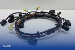
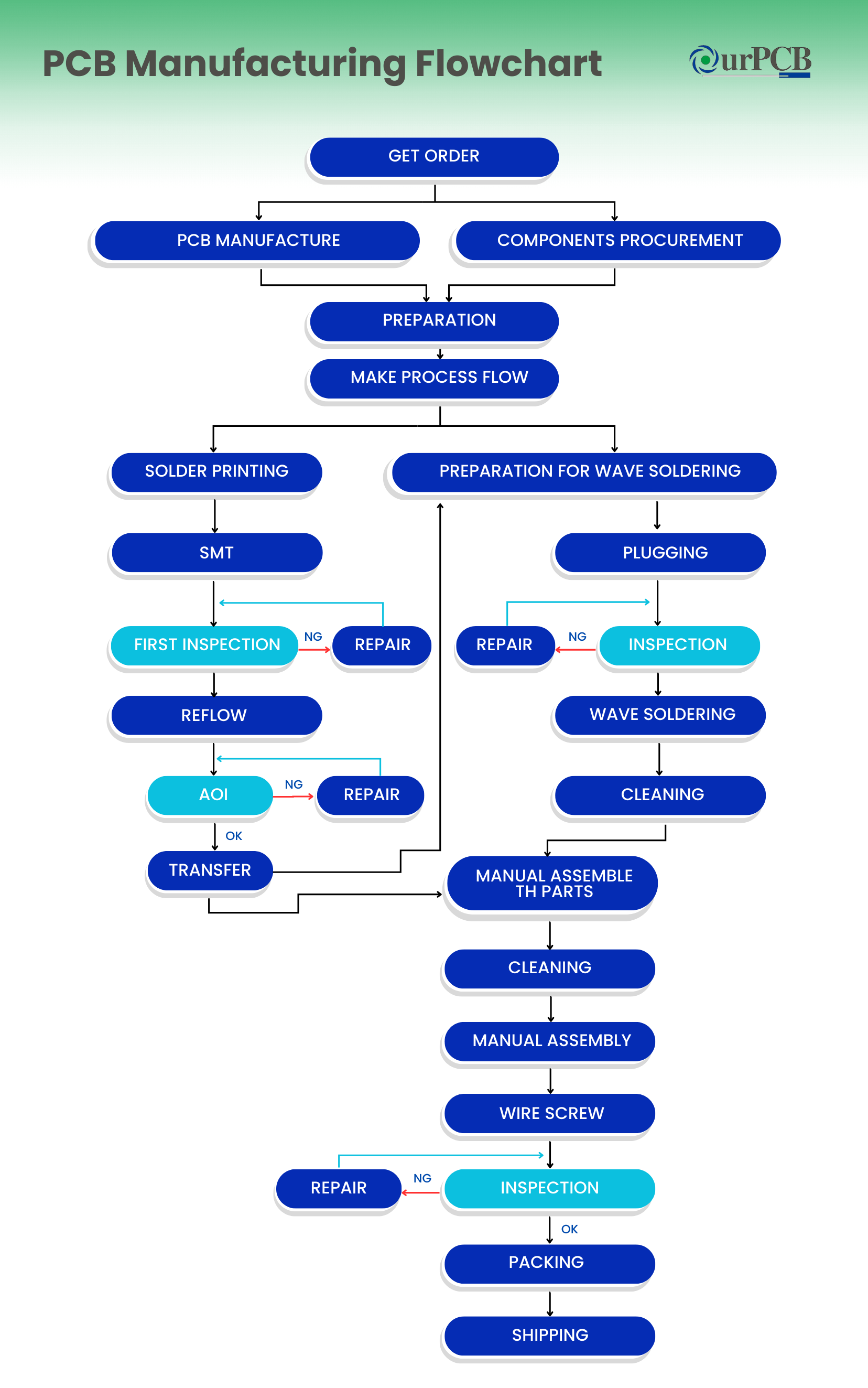
Would your car be able to run without wire harnesses? Not a chance. Wire harnesses connect all the electrical parts together. No harness means no
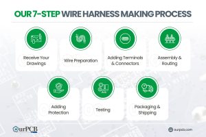
Making wire harnesses isn’t complicated. At OurPCB, we create custom wire harnesses for an expansive range of industries every day. While it’s a complicated process,

Prototype cable assemblies are the very important place in between PCB design ideas and interconnects. OurPCB brings prototype assemblies with PCB solutions to your tables.
PCB thermal management prevents component overheating through strategic heat transfer techniques. Without proper thermal control, electronics are at risk of electronic failures through weakened solder
ContentsKey TakeawaysWhat is a Multilayer-Printed Circuit Board?How do Multilayer PCB Boards Work?Multilayer PCB ApplicationsMultilayer PCB Manufacturing Process: StepsMultilayer PCB Manufacturing MachinesBenefits of Multilayer Circuit BoardsWhat
We use cookies to improve your browsing experience, which may include personal information. By clicking "Agree," you accept our Privacy Policy and cookie use. You can change your cookie settings in your browser anytime.
Agree
 Chat With Us
 Free Quote