Who are the Top 6 Data Cable Manufacturers in China?
When considering the best places for manufacturing data cables, China immediately comes to mind. It’s no surprise either — the country has rapidly ascended in
At OurPCB, we specialize in heavy-copper PCB manufacturing, delivering precision-engineered boards with thick copper layers for high-current applications. We offer multi-layer designs, strict quality control, and expert engineering support to optimize layouts. With industry certifications and a proven track record, we ensure durable, high-performance PCBs.


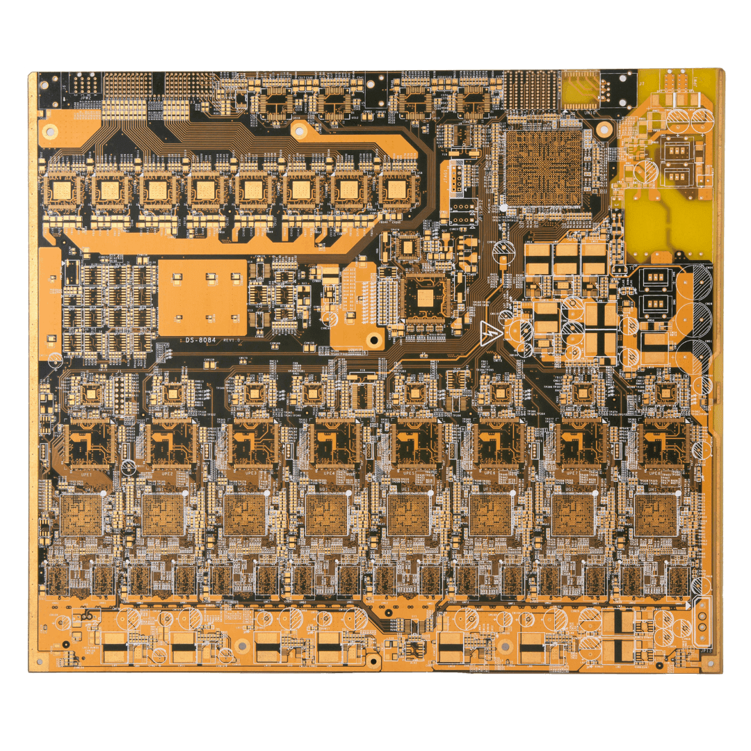


As a specialize heavy copper PCB manufacturer, OurPCB offers comprehensive production capabilities that set us apart from competitors:
| Manufacturing Capability | OurPCB Specifications |
|---|---|
| Copper Thickness | Up to 1000um (with capability for extreme copper needs) |
| Layer Count | 2 – 16 layers |
| Maximum Panel Size | 22.8″ × 18.9″ |
| Aspect Ratio | Maximum 10:1 |
| Minimum Drill Hole | 0.012″ (standard), 0.008″ (specialized) |
| Surface Finishing Options | HASL, OSP, Immersion Gold |
| Base Materials | Aluminum, Polyamide, FR/4 (all TGs), Copper, Ceramic, Teflon |
| Vias | Buried and Blind |
| Quality Standards | IPC 2 Certified |


As a trusted heavy copper PCB manufacturer, our quality assurance department meticulously tests all products before shipment, ensuring flawless performance for your applications:
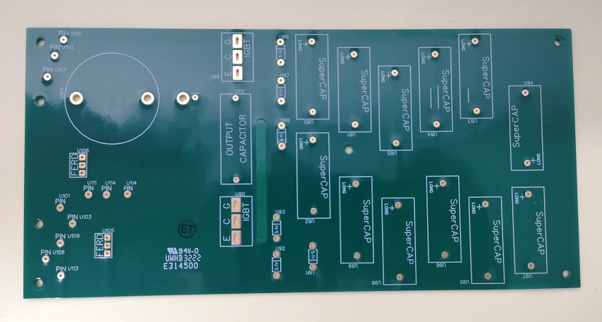

Automated optical inspection detects visual defects
Identifies internal structural issues invisible to the naked eye
Verifies electrical connectivity and performance
Guarantees consistent manufacturing excellence


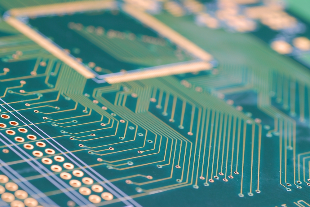
What distinguishes OurPCB as an industry-leading heavy copper PCB manufacturer is our commitment to customer satisfaction:


As an experienced heavy copper PCB manufacturer, OurPCB considers these critical factors during production:
| Baseline Copper Foil Thickness | 105 μm | 140 μm | 175 μm | 210 μm |
|---|---|---|---|---|
| Loss (mils/mm) | ~3/0.08 | ~5/0.13 | ~6/0.15 | ~7/0.18 |
| Minimum Spacing (mils) | 13 | 15 | 20 | 27 |
| Minimum Path Width (mils) | 12 | 14 | 18 | 25 |
Our manufacturing expertise ensures precision across all specifications, including:
Our manufacturing capabilities cover the full spectrum of heavy copper PCB designs:
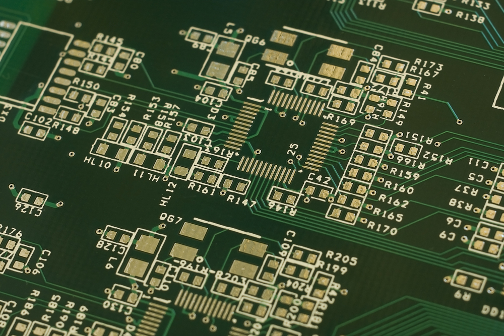

Ideal for LED lighting systems and simple power applications
Perfect for power supplies and more complex devices
Essential for aerospace and advanced electronics
Specialized boards with copper thickness exceeding 1000 μm for industrial transformers
Combining flexibility with heavy copper technology for unique form factors
Integrating standard copper with high-frequency materials for specialized applications
Incorporating high-density interconnect technology for military and advanced applications


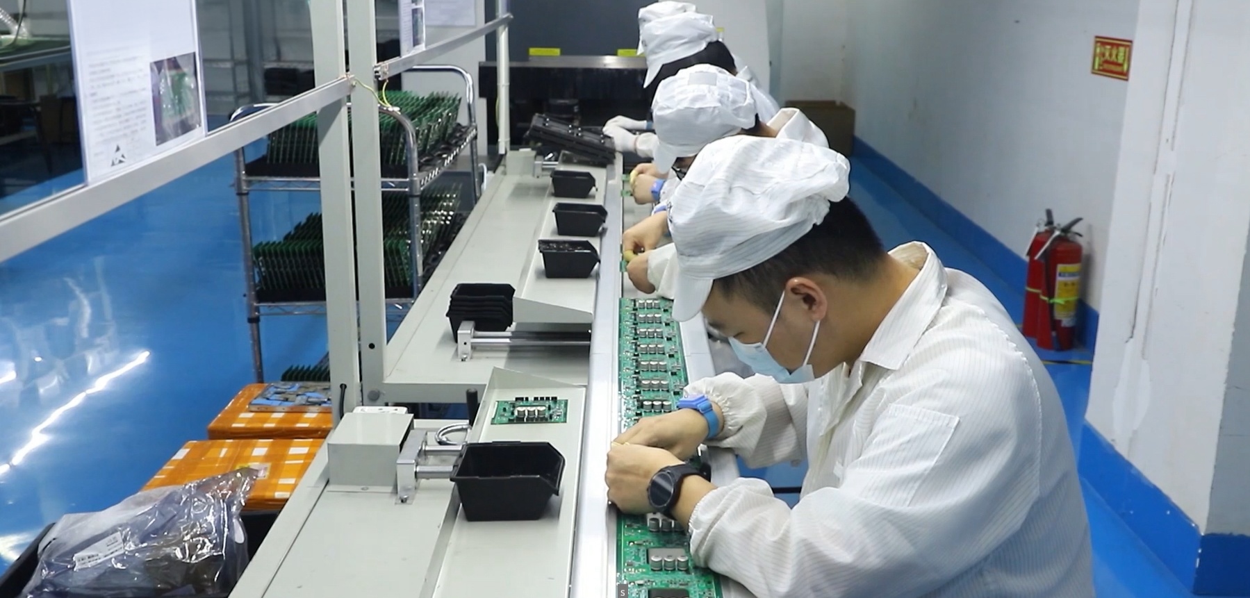
We handle everything from parts sourcing to final assembly, providing a hassle-free experience that ensures top-quality boards every time.

Whether you need a few prototypes or large-volume batches, our flexible assembly services adapt to your project’s scope and timeline.

Stay environmentally responsible with our compliant assembly processes, offering RoHS and lead-free options for safe, reliable builds.

No matter the complexity, we can assemble boards of all configurations—single-layer, multi-layer, or a mix—to match your exact specifications.

From one-off prototypes to bulk orders, we accommodate projects of all sizes without compromising on quality or turnaround time.

Join our growing community of satisfied clients who rely on our dependable assembly expertise and dedicated customer support.


As a premier heavy copper PCB manufacturer, our products deliver significant advantages:


Mon-Fri: 24 hours,
Sat: 9am-6pm, GMT+8

Reach us at
[email protected]
24 hours online

+86-199-30589219
Mon-Fri: 24 hours,
Sat: 9am-6pm, GMT+8
OurPCB specializes in manufacturing heavy copper PCBs with copper thickness ranging from 3 oz to 30 oz per square foot. These PCBs offer superior current-carrying capacity and enhanced thermal management, making them ideal for demanding applications.
OurPCB serves a wide range of industries, including:
With extensive experience and expertise, OurPCB ensures high-performance heavy copper PCBs for critical applications.

When considering the best places for manufacturing data cables, China immediately comes to mind. It’s no surprise either — the country has rapidly ascended in
Finding the right wiring harness manufacturer for your vintage ride can be a real headache. Those beautiful old machines need special wiring that looks period-correct
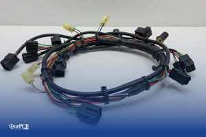
Would your car be able to run without wire harnesses? Not a chance. Wire harnesses connect all the electrical parts together. No harness means no
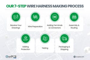
Making wire harnesses isn’t complicated. At OurPCB, we create custom wire harnesses for an expansive range of industries every day. While it’s a complicated process,

Prototype cable assemblies are the very important place in between PCB design ideas and interconnects. OurPCB brings prototype assemblies with PCB solutions to your tables.
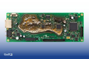
PCB thermal management prevents component overheating through strategic heat transfer techniques. Without proper thermal control, electronics are at risk of electronic failures through weakened solder
We use cookies to improve your browsing experience, which may include personal information. By clicking "Agree," you accept our Privacy Policy and cookie use. You can change your cookie settings in your browser anytime.
Agree