Top 10 Classic Car Wiring Harness Manufacturers | Full Guide
Finding the right wiring harness manufacturer for your vintage ride can be a real headache. Those beautiful old machines need special wiring that looks period-correct

OurPCB provides a controlled PCBA cleaning process that removes flux residue, solder paste contaminants, and ionic debris from the PCBA surface.
Contamination left behind after the soldering process can compromise functionality in high-reliability electronics. Every board is cleaned to meet IPC-A-610 Class 3 cleanliness inspection standards, reducing the risk of electrochemical migration, dendritic growth, and coating adhesion failure.
Whether supporting conformal coating or protecting assemblies in automotive, medical, or industrial systems, we deliver consistent, standards-aligned PCBA cleaning results that maintain long-term performance.


Our PCBA cleaning process removes post-solder contamination that interferes with circuit function, coating adhesion, and long-term reliability.
This includes flux residue, solder paste, and assembly debris such as dust, ink, fingerprints, and oxidation. These materials impact the PCBA surface electrically and mechanically, so they must be removed to maintain coating performance, inspection clarity, and electrical isolation.
Some contaminants, like no-clean flux, absorb moisture and form ionic pathways that trigger electrochemical migration, delamination, or shorts, especially in dense SMT assemblies.
These residues often settle beneath low-standoff parts, where they can’t be verified by visual inspection alone.

We use vapor degreasing to clean fine-pitch SMT assemblies where low standoff heights prevent rinsing under components. The process heats a fluorinated cleaning fluid such as HFE-72DA until it vaporizes at 58 °C.
Our sealed-chamber systems recover 90% of solvent through closed-loop distillation and vapor filtration. Because no water is used, this PCBA cleaning method prevents capillary trapping and delivers dry, spot-free boards that are immediately ready for conformal coating or inspection.
For high-throughput cleaning, we operate fully enclosed aqueous cleaning systems that combine high-pressure spray with saponified deionized water at 60 °C. These systems target assemblies with solder paste, rosin, or water-soluble flux, removing active ions and organic residue from both sides of the board.
Our InJet platforms use 2.0 bar rotary spray heads for impingement and cascade rinsing with resistivity sensors that maintain <1.56 µg/cm² NaCl equivalent. Each cleaned board is force-dried at 70 °C for 10 minutes to eliminate moisture and prepare the surface for optical inspection or downstream processing. This is the most efficient method for batch-based PCBA cleaning at scale.
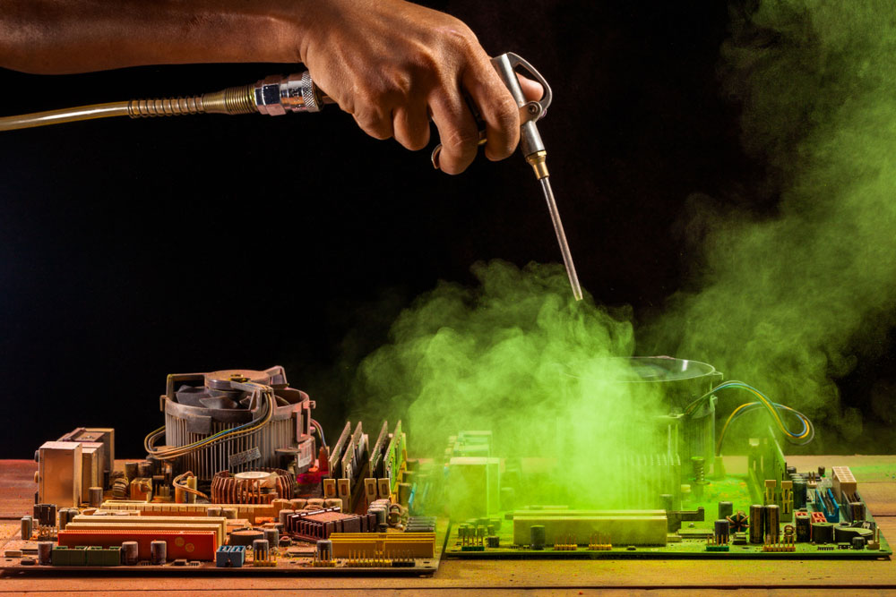
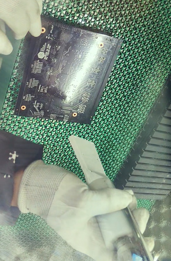
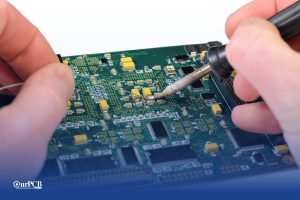
When boards require post-assembly rework or selective soldering, we apply a controlled manual cleaning process to treat localized contamination. Technicians begin by applying Decotron T383 or high-purity IPA to the assembly surface, then scrubbing with anti-static brushes at a 45° angle and 250 g pressure.
Flux is then removed using a directional aerosol rinse, and drying is completed with 30 psi filtered air or lint-free polyester wipes. This method allows us to clean the PCBA without subjecting sensitive components to immersion or thermal stress. We document all manual cleaning steps for traceability on high-reliability builds in automotive, medical, and aerospace programs.
At OurPCB, we remove no-clean flux during the PCBA cleaning process to prevent insulation resistance loss, support coating adhesion, and avoid inspection rejection in Class 2 and 3 assemblies.
Although low-solid no-clean flux is engineered to remain on the board, its residue absorbs moisture, lowers surface resistivity, and disrupts conformal coating uniformity, especially near component edges or mask-defined pads.
Our PCBA cleaning procedures are based on flux type, component density, and coating thickness requirements, and are qualified using ionic cleanliness testing, white residue detection, and surface preparation metrics that ensure coating and inspection compliance.
We remove no-clean flux residue because its remaining solids form hygroscopic films with ionic content capable of enabling leakage currents under bias. These residues often contain halide activators or rosin derivatives that, in humid environments, allow ionic mobility as low as 10⁸ Ω insulation resistance across narrow conductor spacing.
On high-density printed circuit board assemblies, especially those with ≤0.3 mm pitch, this can lead to dendritic growth, moisture-induced tracking, and eventual open or short failures. In Class 3 applications, even visually benign residues violate IPC J-STD-001 Section 8.3.1, prohibiting any visible residue under conformal coating.
Our cleaning strategy depends on the flux chemistry and board design. For fully assembled SMT boards, we use vapor degreasing with HFE-72DA or Vertrel XF, which condense at 55 °C – 65 °C onto the PCBA surface, dissolve polar and non-polar residues, and evaporate without leaving water or exposing components to immersion.
In rework areas or where selective cleaning is required, we use Decotron T383 or high-purity IPA with aerosol precision nozzles to rinse solder ball traps and low-solids residue from around pads.
The process is followed by 30 psi filtered air drying or vacuum-assisted drying to prevent water adsorption beneath packages. Surface prep is validated using surface insulation resistance (SIR) measurements, ionic testing (<1.56 µg/cm² NaCl equivalent), and UV light to detect fluorescence from missed residues.
Removing flux residue allows for consistent conformal coating flow and edge adhesion, especially in boards using urethane or acrylic coatings. Cleaned surfaces increase surface energy, improving film wetting and eliminating common defects like dewetting, bridging, or edge lift.
Coating adhesion strength improves from 1.2 N/mm (on flux-contaminated surfaces) to over 2.5 N/mm on properly cleaned copper and solder mask regions, reducing delamination risk during thermal cycling. In addition, a clean PCB surface ensures that automated optical inspection (AOI), UV inspection, or manual visual checks can accurately detect voids, bubbles, or skipped areas.
For applications in automotive ECUs, implantable medical devices, or high-speed digital RF systems, surface cleanliness before coating directly correlates to long-term device reliability in harsh conditions.
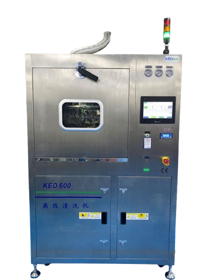
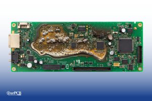
At OurPCB, we use dedicated, precision-controlled PCBA cleaning systems designed to meet IPC Class 2 and Class 3 cleanliness requirements across a range of board types and assembly workflows.
All machines are qualified through validation runs using ionic cleanliness testing and surface inspection to confirm they meet our reliability targets. By combining automated and manual platforms, we deliver consistent cleaning performance across both batch production and selective rework.

At OurPCB, we select cleaning agents based on flux composition, surface compatibility, board sensitivity, and downstream coating requirements. Our fluid systems include water-based cleaning solutions and specialized solvents, each matched to target specific contaminants without damaging solder joints, masks, or exposed metallization.
All chemicals used in our PCBA cleaning process are certified for electronics use and undergo in-house validation for rinseability, drying behavior, and ion content control. This enables consistent performance across batch and localized applications while supporting Class 3 cleanliness requirements.
We use Decotron CP381 as our primary detergent in aqueous batch systems. This fluid is engineered for high-impingement spray cleaning of rosin, no-clean flux, and solder paste residues.
Formulated for low foaming and high rinsability, it maintains cleaning effectiveness across a temperature range of 50 °C to 70 °C while remaining stable in closed-loop wash tanks.
CP381 supports saponification of organic acids and resin binders, enabling complete residue breakdown without masking inspection surfaces.
We monitor conductivity before and after rinsing to confirm agent removal and prevent redeposition.
We use HFE-72DA and Vertrel XF in our vapor-phase systems to dissolve polar and non-polar flux residue beneath low-standoff components.
These fluids have boiling points in the 55 °C to 65 °C range, low surface tension, and fast drying characteristics that leave boards immediately ready for conformal coating.
For localized or rework cleaning, we use Decotron T383 and 99% IPA in combination with directional aerosol dispensers and antistatic brushes.
T383 is selected for its halide-free formulation, high evaporation rate, and non-damaging profile across exposed copper, gold fingers, and sensitive dielectric surfaces.
At OurPCB, we validate each PCBA cleaning process by confirming that all ionic contaminants, flux residue, and post-cleaning films have been eliminated to a level that supports downstream coating, signal stability, and long-term electrical integrity.
We do this across all production batches and reworked assemblies, especially when boards are destined for regulated or high-stress environments.
Our approach uses surface analysis, insulation testing, and full traceability to confirm that each board meets IPC Class 2 and 3 reliability expectations. This verification step is a required part of every high-reliability electronics build we support.
We inspect coating adhesion by evaluating surface condition, film bonding strength, and visual cleanliness.
Boards undergo cross-hatch tape testing and edge pullback verification to confirm that coatings bond cleanly over mask and metal features.
Measured adhesion strength must exceed 2.5 N/mm in test zones across the board surface to avoid delamination under thermal or mechanical stress.
We also use UV trace detection and angled light inspection at 10x magnification to identify retained no-clean flux or whitening near pad edges.
These steps confirm that the surface is free of residues that could disrupt coating coverage or adhesion.
To validate electrical reliability, we run surface insulation resistance (SIR) tests and biased humidity screening across cleaned assemblies.
Boards are subjected to 85 °C/85% RH for 168 hours while energized at 5 VDC to simulate moisture-driven current paths. If cleaning is incomplete, we detect leakage below 10⁸ Ω or observe dendritic growth between fine-pitch nets.
These tests are applied to confirm the removal of water-reactive residue, particularly around RF shielding points, connector arrays, and coated signal paths.
They allow us to qualify each PCBA cleaning process for analog circuits, sensor lines, and high-speed digital routing.

We maintain full traceability of each cleaned assembly using system-logged data and process-linked documentation. Parameters such as temperature, airflow, solvent concentration, and rinse resistivity are stored per lot and linked to a build reference code.
This allows us to verify that every board received consistent quality cleaning, detect process drift, and respond to field investigations when required. These records are mandatory in automotive, medical, and aerospace programs where long-term compliance, audit response, and build reproducibility are part of the project deliverables.
OurPCB helps engineers and procurement teams resolve PCB signal integrity problems before fabrication by offering detailed design review, material compatibility checks, and stackup validation.
We work with you to identify potential problems in impedance matching, return current routing, and via transitions that could cause signal degradation or failure in timing-sensitive applications.
We manage every stage of the PCBA cleaning process, from method selection to final inspection and traceable documentation.
This includes pairing cleaning systems with flux type, verifying solvent compatibility, and confirming residue removal through NaCl-equivalent testing.
Each batch is run under validated parameters and logged with equipment profile, cycle time, and chemistry records.
We clean no-clean flux and lead-free solder residues from boards with low standoff height, sensitive components, or hybrid SMT/THT layouts.
Vapor-phase degreasing and selective benchtop processes are used, depending on residue type and downstream coating or inspection needs.
These methods are validated for conformal coating, underfill, and high-impedance surface readiness.
We support Class 2 and Class 3 cleaning for boards used in automotive, medical, aerospace, and mission-critical embedded control systems.
Cleaning reliability is verified through insulation resistance testing, white residue inspection, and SIR protocol results when required.
Our team prepares records for each lot with cleaning steps, test results, and image evidence when applicable.

We select each cleaning agent based on flux chemistry and surface compatibility. CP381 is used for water-soluble fluxes in pressurized aqueous systems, while HFE-based solvents and Decotron T383 are applied for halide-free or low-solid residues.
Each fluid is tested against surface finish, solder mask integrity, and coating compatibility for predictable performance.
Our cleaning systems include InJet 388, AirJet 594, and INJET 888 CRRD platforms optimized for multi-sided spray cleaning, batch capacity, and part fixture flexibility.
We configure each platform for component height, board format, and contamination profile using adjustable pressure, heat, and rinse cycle parameters. Closed-loop filtration and programmable cycles support repeatability across product types.
Mon-Fri: 24 hours,
Sat: 9am-6pm, GMT+8
Reach us at
[email protected]
24 hours online
+86-199-30589219
Mon-Fri: 24 hours,
Sat: 9am-6pm, GMT+8
Cleaning “no-clean” flux is recommended when electrical stability, surface preparation, or downstream testing could be affected by film formation or conductive traces. These materials may leave behind hygroscopic compounds that attract moisture and reduce insulation, even if their visual profile appears benign.
Removing them with the correct cleaning solution reduces the risk of current leakage, improves coating adhesion, and helps maintain inspection clarity. For a clean PCB to be accepted in high-performance environments, post-process film removal is often necessary, regardless of initial flux classification.
Electrochemical migration occurs when moisture, surface ions, and electrical bias interact on a circuit board and trigger unwanted conductive growth. The process begins with metal dissolution at the anode, where copper atoms release into a thin film of surface moisture.
These ions then undergo ion migration, moving toward the cathode along the moisture path. Finally, dendrite growth occurs at the cathode, where the metal ions deposit and form conductive filaments between traces.
PCBA cleaning removes ionic contaminants that make this process possible, especially in high-humidity environments or boards with tightly spaced conductors.
Acceptable contamination levels are defined by industry standards such as IPC J-STD-001, which specifies limits based on ionic content and surface area.
Most manufacturers target less than 1.56 µg/cm² NaCl equivalent using resistivity of solvent extract (ROSE) testing. Some designs use SIR testing to simulate in-use conditions over time, while others require full surface rinse validation to confirm that ionic films have been entirely removed.
For surface coatings to perform correctly, a clean PCBA must meet both ionic and visual thresholds before final packaging.
The best PCBA cleaning method depends on board density, component standoff height, and surface accessibility. For fine-pitch layouts and bottom-terminated packages, vapor-phase degreasing using low surface tension cleaning chemicals is often the most effective.
Boards with moderate spacing and compatible materials may be cleaned in high-pressure water-based batch systems using saponified fluid and deionized water. The cleaning method must match the design’s geometry and thermal tolerance to prevent trapped fluid or incomplete surface preparation.
Ultrasonic cleaning uses high-frequency sound waves, typically around 40 kHz, to create microscopic cavitation bubbles in a cleaning solution. As these bubbles collapse near the surface of the printed circuit, they dislodge contamination from under components and within narrow gaps.
This technique is especially useful for removing debris around dense connector arrays, low standoff components, or shielded modules. To avoid part damage, the process is tuned for fluid type, frequency, and exposure time, with post-process drying used to eliminate any retained moisture.
Vapor degreasing should be used when physical access is limited or moisture-sensitive components make water-based systems unsuitable. It condenses heated solvent vapor onto a cooler printed circuit board, dissolving contaminants without liquid immersion.
Because it leaves no water, vapor degreasing is ideal for boards requiring rapid drying, minimal residue, and immediate readiness for conformal coating or testing. The method also benefits reflowed assemblies with tight lead spacing and uncoated copper.
PCBA cleanliness is governed by IPC-J-STD-001, which sets criteria for post-solder cleaning requirements and contamination thresholds. Section 8.3 defines when cleaning is required and outlines acceptable residue limits and visual inspection rules.
Validation is performed using methods referenced in IPC-TM-650, including ROSE (resistivity of solvent extract) and SIR (surface insulation resistance) testing. For high-performance designs, Class 3 requirements demand tighter contamination control than Class 2, especially for coating adhesion and long-term electrical isolation.
Selective cleaning targets only the soldered region without exposing the rest of the board to full-system wash cycles. This is done by applying a directional cleaning solution to the affected area using controlled fluid delivery, agitation, and low-pressure rinse.
Operators isolate the region to prevent solvent migration and use air-assisted drying to avoid trapping moisture. The process is proper after hand-insertion or post-test repairs, where full immersion may damage sensitive components or coatings.
Contamination failures may present as field returns with intermittent behavior, dielectric breakdown, or unexpected conduction paths between circuit nodes. Diagnostic tests show low insulation resistance, leakage during humidity exposure, or dendritic bridging visible under magnification.
Physical indicators include staining, crystalline films, or darkened areas around pad edges. Failures often appear after thermal cycling, humidity aging, or long-term bias testing.
Yes, remaining films on the surface interfere with the wetting and adhesion properties of conformal coatings. These films reduce surface energy, resulting in poor flow, edge beading, or gaps between lead exits and the mask.
When coatings lift or pull back during curing or thermal cycling, unprotected metal can become exposed. For optimal bonding, the board surface must be clean, dry, and free from interference before any coating is applied.
Contact OurPCB to schedule a PCBA cleaning consultation or submit your build files for a validated quote. We’ll match your design, flux type, and coating process with a cleaning workflow that meets IPC standards and delivers consistent performance.
Finding the right wiring harness manufacturer for your vintage ride can be a real headache. Those beautiful old machines need special wiring that looks period-correct
Would your car be able to run without wire harnesses? Not a chance. Wire harnesses connect all the electrical parts together. No harness means no
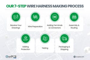
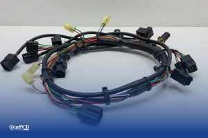
Making wire harnesses isn’t complicated. At OurPCB, we create custom wire harnesses for an expansive range of industries every day. While it’s a complicated process,
Prototype cable assemblies are the very important place in between PCB design ideas and interconnects. OurPCB brings prototype assemblies with PCB solutions to your tables.
PCB thermal management prevents component overheating through strategic heat transfer techniques. Without proper thermal control, electronics are at risk of electronic failures through weakened solder
ContentsKey TakeawaysWhat is a Multilayer-Printed Circuit Board?How do Multilayer PCB Boards Work?Multilayer PCB ApplicationsMultilayer PCB Manufacturing Process: StepsMultilayer PCB Manufacturing MachinesBenefits of Multilayer Circuit BoardsWhat
We use cookies to improve your browsing experience, which may include personal information. By clicking "Agree," you accept our Privacy Policy and cookie use. You can change your cookie settings in your browser anytime.
Agree
 Chat With Us
 Free Quote