Top 10 Classic Car Wiring Harness Manufacturers | Full Guide
Finding the right wiring harness manufacturer for your vintage ride can be a real headache. Those beautiful old machines need special wiring that looks period-correct
 5 Star Rating on

OurPCB manufactures high-precision PCBs with 2 mil outer layer line spacing, ±0.025 mm drill alignment accuracy, and copper thicknesses up to 12 oz.
We support up to 50 layers across rigid, flex, and rigid-flex designs using FR4, PTFE, PPO/PPE, and ceramic-filled substrates.
All PCB assemblies meet IPC-6012 Class 2 or 3, ISO 9001, IATF 16949, and RoHS requirements.


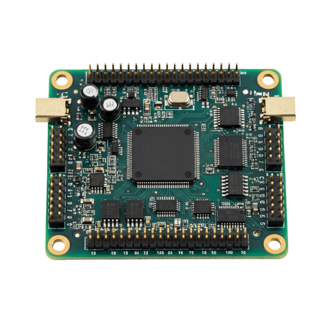


At OurPCB, high-end precision PCB services are defined by trace-level feature control, via registration accuracy, and material-specific manufacturing workflows. We support up to 50-layer stackups with tight copper uniformity, 2 mil outer layer trace geometry, and ±0.025 mm optical drill alignment.
These tolerances are required for high-speed digital signals, impedance-controlled designs, and thermally constrained assemblies across HDI, RF, and rigid-flex formats. We deliver full production traceability for every China high precision multilayer PCB order, from imaging to final test.

We structure all precision PCB services around matched lamination, plating, and imaging sequences designed to maintain registration across the full layer stack. For all our precision multilayer PCB orders, we support up to 8 sequential lamination cycles with process conditions tailored to the material’s resin system, Z-axis expansion, and glass transition temperature.
Each cycle is programmed with vacuum application, heating slope, pressure dwell, and cooldown matched to FR4, PTFE, PPO/PPE, or ceramic-filled substrates. Controlled copper plating is applied using area-specific current densities and bath profiles based on target thickness, via depth, and pad geometry.
We support up to 12 oz copper for outer layers and maintain plating uniformity within ±10% using real-time thickness monitoring and in-panel reference coupons. For via structures, our precision PCB process enforces a minimum 1 mil copper barrel thickness and defines thermal relief or solid connection patterns during CAM review. Every parameter is defined, recorded, and confirmed by MES, with full traceability assigned to each panel from layup to inspection.
We use laser-guided drill targeting and surface-to-core alignment correction systems to maintain dimensional control in every precision PCB. Our optical registration workflow begins with LDI image capture aligned to etched fiducials, with drill pattern compensation applied for material shrinkage and tooling tolerance. Laser microvias are drilled at 3 to 6 mil diameters, with Z-axis registration validated by camera overlay and fiducial-based trace recalibration.
We run alignment sampling across panel quadrants and compensate drill positions using image-to-drill feedback captured during production. For Class 3 jobs, we enforce trace-to-hole registration limits of ±25 microns, with pass/fail thresholds for concentricity across pad arrays.
Fine-line features on 8 μm base copper are shaped using resist edge profile control and verified post-etch using inspection targets on outer layers. These alignment systems are critical for maintaining electrical length uniformity and controlling reflection points in high-speed differential pairs.
All precision PCB services involving stacked microvias, fine-pitch QFNs, or HDI build-up are processed with this control model. All drill alignment, etch imaging, and feature distortion metrics are recorded for final-layer inspection and panel-level review.
We manage every layer stack based on material compatibility, press cycle sequencing, and Z-axis expansion modeling to ensure structural stability and electrical performance. Our engineering team defines each precision PCB service with pre-qualified dielectric systems including FR4, high-Tg FR4, halogen-free epoxy, PPO/PPE blends, ceramic-filled PTFE, and hybrid multilayer arrangements.
For precision PCB services, stackup geometry is defined during CAM using material-specific thickness profiles and prepreg resin content.
We support up to 50 rigid layers and 30 rigid-flex layers with lamination press cycles assigned according to resin melt point, curing kinetics, and flow direction. Low-flow prepregs and bonding films are matched to core roughness and copper topography to eliminate delamination or voiding.
Each press pass is logged with thermal expansion tracking and post-press inspection of dielectric spacing and layer-to-layer alignment. All high-precision PCB builds undergo interlayer verification using X-ray registration targets and microsection evaluation to confirm uniformity and mechanical stack compliance.
For builds requiring mixed substrates, we validate expansion behavior across material transitions and apply resin damming or copper compensation layers as required. These material coordination processes are foundational to our ability to manufacture complex, impedance-stable, and thermally balanced precision PCBs.
OurPCB configures thermal profiles for each precision assembly based on solder alloy type, PCB thickness, component density, and substrate material. We support SAC305, Sn63/Pb37, low-temperature SnBi, and high-mass lead-free alloys with reflow profiles tuned across four to seven zones.
Ramp rates are held between 1.0 and 3.0 °C/sec with soak temperatures ranging from 150 to 180 °C and peak temperatures of 235 to 250 °C, depending on alloy class. Convection reflow is performed with or without nitrogen, and all profiles are verified against thermocouple data collected from thermal test vehicles or dummy boards representing maximum thermal load.
For double-sided assemblies, we apply adhesive dotting or low-tack underfill during the first pass and adjust soak/peak times in the second reflow to prevent joint collapse. Large BGAs and QFNs are modeled for heat sink effect and delta-T across the package, and auxiliary preheaters are used on thick boards to reduce warp and solder voiding. For boards with mixed-technology components, we use selective soldering with radiant preheating to 100 to 120 °C and nozzle dwell times controlled to ±0.5 sec for consistent joint fill.
Thermal stress-sensitive parts, including ceramic capacitors and crystal oscillators, are flagged in the CAM database and assigned reduced ramp rates or external shielding during reflow. All reflow ovens are profiled and validated regularly with a 6-point thermocouple array to confirm zone consistency and peak overshoot tolerances.


At OurPCB, high-end precision PCB services are defined by trace-level feature control, via registration accuracy, and material-specific manufacturing workflows. We support up to 50-layer stackups with tight copper uniformity, 2 mil outer layer trace geometry, and ±0.025 mm optical drill alignment.
These tolerances are required for high-speed digital signals, impedance-controlled designs, and thermally constrained assemblies across HDI, RF, and rigid-flex formats. We deliver full production traceability for every China high precision multilayer PCB order, from imaging to final test.

We structure all precision PCB services around matched lamination, plating, and imaging sequences designed to maintain registration across the full layer stack. For all our precision multilayer PCB orders, we support up to 8 sequential lamination cycles with process conditions tailored to the material’s resin system, Z-axis expansion, and glass transition temperature.
Each cycle is programmed with vacuum application, heating slope, pressure dwell, and cooldown matched to FR4, PTFE, PPO/PPE, or ceramic-filled substrates. Controlled copper plating is applied using area-specific current densities and bath profiles based on target thickness, via depth, and pad geometry.
We support up to 12 oz copper for outer layers and maintain plating uniformity within ±10% using real-time thickness monitoring and in-panel reference coupons. For via structures, our precision PCB process enforces a minimum 1 mil copper barrel thickness and defines thermal relief or solid connection patterns during CAM review. Every parameter is defined, recorded, and confirmed by MES, with full traceability assigned to each panel from layup to inspection.

We use laser-guided drill targeting and surface-to-core alignment correction systems to maintain dimensional control in every precision PCB. Our optical registration workflow begins with LDI image capture aligned to etched fiducials, with drill pattern compensation applied for material shrinkage and tooling tolerance. Laser microvias are drilled at 3 to 6 mil diameters, with Z-axis registration validated by camera overlay and fiducial-based trace recalibration.
We run alignment sampling across panel quadrants and compensate drill positions using image-to-drill feedback captured during production. For Class 3 jobs, we enforce trace-to-hole registration limits of ±25 microns, with pass/fail thresholds for concentricity across pad arrays.
Fine-line features on 8 μm base copper are shaped using resist edge profile control and verified post-etch using inspection targets on outer layers. These alignment systems are critical for maintaining electrical length uniformity and controlling reflection points in high-speed differential pairs.
All precision PCB services involving stacked microvias, fine-pitch QFNs, or HDI build-up are processed with this control model. All drill alignment, etch imaging, and feature distortion metrics are recorded for final-layer inspection and panel-level review.
We manage every layer stack based on material compatibility, press cycle sequencing, and Z-axis expansion modeling to ensure structural stability and electrical performance. Our engineering team defines each precision PCB service with pre-qualified dielectric systems including FR4, high-Tg FR4, halogen-free epoxy, PPO/PPE blends, ceramic-filled PTFE, and hybrid multilayer arrangements.
For precision PCB services, stackup geometry is defined during CAM using material-specific thickness profiles and prepreg resin content.
We support up to 50 rigid layers and 30 rigid-flex layers with lamination press cycles assigned according to resin melt point, curing kinetics, and flow direction. Low-flow prepregs and bonding films are matched to core roughness and copper topography to eliminate delamination or voiding.
Each press pass is logged with thermal expansion tracking and post-press inspection of dielectric spacing and layer-to-layer alignment. All high-precision PCB builds undergo interlayer verification using X-ray registration targets and microsection evaluation to confirm uniformity and mechanical stack compliance.
For builds requiring mixed substrates, we validate expansion behavior across material transitions and apply resin damming or copper compensation layers as required. These material coordination processes are foundational to our ability to manufacture complex, impedance-stable, and thermally balanced precision PCBs.
OurPCB configures thermal profiles for each precision assembly based on solder alloy type, PCB thickness, component density, and substrate material. We support SAC305, Sn63/Pb37, low-temperature SnBi, and high-mass lead-free alloys with reflow profiles tuned across four to seven zones.
Ramp rates are held between 1.0 and 3.0 °C/sec with soak temperatures ranging from 150 to 180 °C and peak temperatures of 235 to 250 °C, depending on alloy class. Convection reflow is performed with or without nitrogen, and all profiles are verified against thermocouple data collected from thermal test vehicles or dummy boards representing maximum thermal load.
For double-sided assemblies, we apply adhesive dotting or low-tack underfill during the first pass and adjust soak/peak times in the second reflow to prevent joint collapse. Large BGAs and QFNs are modeled for heat sink effect and delta-T across the package, and auxiliary preheaters are used on thick boards to reduce warp and solder voiding. For boards with mixed-technology components, we use selective soldering with radiant preheating to 100 to 120 °C and nozzle dwell times controlled to ±0.5 sec for consistent joint fill.
Thermal stress-sensitive parts, including ceramic capacitors and crystal oscillators, are flagged in the CAM database and assigned reduced ramp rates or external shielding during reflow. All reflow ovens are profiled and validated regularly with a 6-point thermocouple array to confirm zone consistency and peak overshoot tolerances.
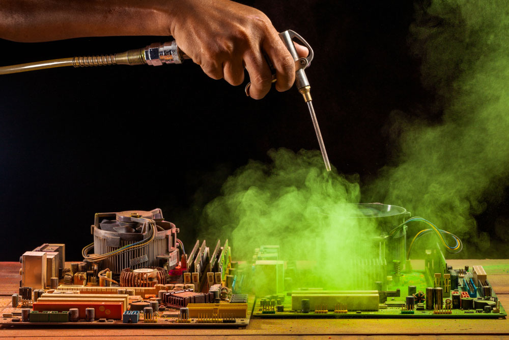
At OurPCB, we remove no-clean flux during the PCBA cleaning process to prevent insulation resistance loss, support coating adhesion, and avoid inspection rejection in Class 2 and 3 assemblies.
Although low-solid no-clean flux is engineered to remain on the board, its residue absorbs moisture, lowers surface resistivity, and disrupts conformal coating uniformity, especially near component edges or mask-defined pads.
Our PCBA cleaning procedures are based on flux type, component density, and coating thickness requirements, and are qualified using ionic cleanliness testing, white residue detection, and surface preparation metrics that ensure coating and inspection compliance.
We remove no-clean flux residue because its remaining solids form hygroscopic films with ionic content capable of enabling leakage currents under bias. These residues often contain halide activators or rosin derivatives that, in humid environments, allow ionic mobility as low as 10⁸ Ω insulation resistance across narrow conductor spacing.
On high-density printed circuit board assemblies, especially those with ≤0.3 mm pitch, this can lead to dendritic growth, moisture-induced tracking, and eventual open or short failures. In Class 3 applications, even visually benign residues violate IPC J-STD-001 Section 8.3.1, prohibiting any visible residue under conformal coating.
Removing these residues is required to maintain dielectric performance and prevent latent field degradation.
Our cleaning strategy depends on the flux chemistry and board design. For fully assembled SMT boards, we use vapor degreasing with HFE-72DA or Vertrel XF, which condense at 55 °C – 65 °C onto the PCBA surface, dissolve polar and non-polar residues, and evaporate without leaving water or exposing components to immersion.
In rework areas or where selective cleaning is required, we use Decotron T383 or high-purity IPA with aerosol precision nozzles to rinse solder ball traps and low-solids residue from around pads.
The process is followed by 30 psi filtered air drying or vacuum-assisted drying to prevent water adsorption beneath packages. Surface prep is validated using surface insulation resistance (SIR) measurements, ionic testing (<1.56 µg/cm² NaCl equivalent), and UV light to detect fluorescence from missed residues.
Removing flux residue allows for consistent conformal coating flow and edge adhesion, especially in boards using urethane or acrylic coatings. Cleaned surfaces increase surface energy, improving film wetting and eliminating common defects like dewetting, bridging, or edge lift.
Coating adhesion strength improves from 1.2 N/mm (on flux-contaminated surfaces) to over 2.5 N/mm on properly cleaned copper and solder mask regions, reducing delamination risk during thermal cycling. In addition, a clean PCB surface ensures that automated optical inspection (AOI), UV inspection, or manual visual checks can accurately detect voids, bubbles, or skipped areas.
For applications in automotive ECUs, implantable medical devices, or high-speed digital RF systems, surface cleanliness before coating directly correlates to long-term device reliability in harsh conditions.

Our precision PCB services support complex builds requiring non-standard materials, precise dimensional tolerances, and dense interconnect routing. We fabricate multilayer boards with advanced copper, drilling, lamination, and imaging controls that support high-density, high-speed, and hybrid circuit designs.
These capabilities are integrated across two 10,000 m² production facilities using camera-based tooling, automated inspection, and CAM-defined process models for trace geometry, dielectric flow, and registration precision.

OurPCB forms fine copper features using high-resolution laser direct imaging (LDI) aligned to inner-layer fiducials within ±20 μm overlay tolerance. Line widths of 2.0 mil on 25 μm copper are processed with copper expansion factors based on etch rate, laminate shrinkage, and current density across the panel.
Every trace is AOI-scanned pre-lamination using 10 μm resolution optics with defect capture thresholds down to 25 μm for nicks, opens, or bridging. Layer-specific CAM files assign different etchback values per trace class, based on trace impedance, routing length, and field copper density.
Inner layers in a 16-layer stack are processed on separate tooling layers to correct for resin flow and post-laminate drift. Feature distortion, trace angle accuracy, and edge profile are verified by microsection, while mask alignment is confirmed using stepped test structures. These controls protect every circuit, validate inspection data before press, and ensure geometry accuracy through every trace path in the layer stack.

We drill mechanically down to 0.10 mm with ±0.025 mm accuracy using X-ray referenced drill tables and optical registration overlays, with calibration confirmed every 50 panels. Multi-depth drilling for buried via builds is sequenced using build-specific drill stacks and positional offsets programmed at each lamination stage.
Laser microvias are drilled between 3 and 6 mil in diameter using frequency-tuned CO₂ lasers with Z-axis energy control to limit tapering on glass-reinforced PTFE layers. Each via is validated through microsection for barrel roundness, wall collapse, and base resin distortion.
Stacked via assemblies are plated between lam cycles with 1 mil minimum copper wall thickness, then cross-sectioned for concentricity and fill coverage. Blind vias are impedance-profiled using layer-pair impedance coupons placed along routing-critical nets.
Final drill-to-copper clearance is confirmed using AOI and backlighting alignment tables. Every drill operation is fully recorded for MES-based traceability, layer pairing, and routing coverage.

We press up to 8 lamination cycles per job, with full thermal profiling of each pass. Ramp rate is controlled at 2–4 °C/min, stays at 180 to 220 °C for 60 to 90 minutes depending on resin system, and final thickness targets are verified using micrometer and X-ray profile overlays.
Low-flow prepregs are applied between filled cores for HDI builds and resin content is matched to glass style (e.g. 106, 1080, 2113) and copper roughness. Mixed-material layer stack designs using PTFE, PPO/PPE, and epoxy are pressed in sequence with vacuum holding at –950 mbar for 15 minutes.
Core movement, layer shift, and copper exposure at outer layer interfaces are measured by post-laminate cross-section. We apply resin damming films and flow arrest zones for hybrid edge alignment and microvia capture.
All process parameters, including temperature curve, pressure profile, and vent timing, are logged per part number. Press deformation, post-cure bondline, and component footprint distortion are flagged during review and inspection.

Our precision PCB services extend to assembly, using high-speed SMT lines, programmable selective soldering, and multi-zone reflow ovens configured for leaded and lead free processes.
Our placement systems support package sizes down to 01005 with ±0.05 mm accuracy and are optimized for BGAs, QFNs, LGAs, and 0.3 mm pitch fine-pitch components. Solder paste is applied using stainless steel stencils matched to pad geometry, followed by SPI (Solder Paste Inspection) using 3D profilometry to verify height, volume, and alignment before placement.
Pick-and-place machines are programmed with fiducial recognition, component rotation, and package height profiles to maintain vertical coplanarity during high-speed operation. Assemblies with double-sided placement are supported using adhesive tacking or sequential reflow with matched soak and ramp rates to limit solder joint collapse.
Reflow profiles are defined by alloy type (Sn63/Pb37, SAC305, or low-temp SnBi systems), board mass, and component thermal capacity, with nitrogen-assisted convection reflow available for Class 3 assemblies. Selective soldering is used on mixed-technology boards with clearance-limited areas, applying preheat to 100 to 120 °C and programmable nozzle movement at ±0.3 mm repeatability.

OurPCB sources components through approved suppliers, including Digi-Key, Mouser, Future Electronics, and WPG Holdings, to maintain traceability, authenticity, and lifecycle visibility across all precision builds.
Each Bill of Materials (BOM) is verified for part number, footprint, and RoHS compliance prior to procurement, and lifecycle status is cross-referenced against parametric databases to flag end-of-life or NRND parts before ordering. Where alternates are needed, our engineering team performs electrical and mechanical equivalency reviews before substitution.
Optical and X-ray screening is performed on select lots to detect counterfeits, re-marked ICs, or second-hand inventory. Component reels are tracked via barcode or QR labeling through MES, with per-job traceability for quantity, date code, and feeder position assignment.
For consigned kits, OurPCB performs full incoming verification and part count reconciliation. Inventory is handled in FIFO rotation, and traceability is extended to reference designator-level consumption data when required for regulated or high-reliability sectors.

OurPCB maintains full ESD (Electrostatic Discharge) and MSD (Moisture Sensitive Device) controls across all precision PCB assembly lines. ESD protection is enforced through wrist strap monitoring, conductive flooring, ionization bars at pick-and-place feeders, and ESD-safe benches rated to ANSI/ESD S20.20.
All workstations are grounded to <10⁶ ohms, and operators are trained to IPC-A-610E and JEDEC JESD625 standards for ESD control and safe component handling.
MSL-classified components are tracked from inbound receipt using barcode labels that include MSL rating, date code, and dry pack expiration. Devices classified as MSL 2 or higher are stored in dry cabinets at <5% RH or nitrogen boxes with automated RH alarms. Floor life timers are reset through JEDEC-standard baking cycles, at 125 °C for 24 to 48 hours based on device class and exposure time. Reflow entry checks include visual inspection of MSL labels, humidity indicator cards, and package condition.
Moisture-sensitive components flagged in the BOM are automatically routed to nitrogen staging areas between SMT and reflow. Desiccant levels, humidity levels, and bake/rebake cycles are logged against part number in MES and included in final shipment documentation when required.
ESD and MSD compliance audits are performed weekly, and all packaging meets JEDEC and IEC 61340 standards for static shielding and moisture barrier protection.

Copper plating is performed in programmable bath lines with 3-segment panel loading and 12-station electrolyte control. Current density is regulated to 15 to 25 ASF based on hole diameter and field exposure. We control plating uniformity within ±10% across the entire panel, verified using in-panel ring test coupons.
ENIG and ENEPIG finishes are deposited using electroless chemistry with gold thickness from 1 to 3 μin on a 120 μin nickel base. OSP coatings are processed at 40 to 60 °C with oxide film integrity verified through wetting angle and solder ball test.
Hard gold for fingers is applied by electrolytic process with beveling at 30 to 45° using programmable edge cutters. All mask alignment is verified using LDI with reference to final drill data and solder pad positioning.
Post-finish AOI uses 15 μm optics with overlay matching to confirm pad edge coverage and mask clearance. Final imaging data is archived per panel for downstream inspection and post-rework validation if required.

AOI is performed after all primary stages: inner layer etch, outer layer imaging, solder mask, and surface finish. Each AOI station uses cameras with 5 to 10 μm resolution and can detect trace neckdowns, pad deformation, and copper smear.
Microsection inspection is performed on every lot, with pull locations defined in high-density and edge-mount zones. The thickness of dielectric, copper plating, and solder mask are all measured using optical and mechanical gauges and stored against panel ID in our MES.
Electrical testing uses a flying probe at 100 to 250 μm pitch and verifies connectivity, isolation, and resistance per net class. For differential pairs, signal trace impedance is validated using TDR coupons with launch delay and phase shift compared to simulation.
All test failures are logged with trace origin, and boards requiring rework are routed through controlled workstations under Class 3 IPC criteria. Every test step in our precision PCB services links back to the original circuit ID and job number.

Our precision PCB services are certified to ISO 9001, IATF 16949, and products to IPC-6012 Class 2 and 3. All certifications are logged at the job setup stage and assigned to the production traveler. Each build includes documented inspection, test, and cross-section checkpoints tied to the job ID and panel number.
Certifications are validated at the final stage using inspection signoffs, solderability verification, impedance report summary, and visual acceptance forms. RoHS compliance is supported using lead-free solder alloys, halogen-free prepregs, and ENIG/OSP finishes. Internal documentation is archived for trace audit and sent to customers on request through COC, microsection data, and electrical test reports.
Each panel’s routing data, testing results, and drill performance record are stored in MES for trace review and complaint resolution. Certification criteria are applied regardless of job type, prototype, volume, or engineering validation.


Our precision PCB services include advanced BGA services for production and post-assembly correction of high-density packages, including standard BGA, microBGA, LGA, PoP (Package-on-Package), and CSP. All BGA rework services and reballing operations are performed using split-vision BGA rework stations with ±0.025 mm placement accuracy and programmable thermal profiling.
Site removal uses localized hot air or infrared heating with automatic nozzle height calibration, thermocouple feedback, and component-specific soak and peak profiles.

Mon-Fri: 24 hours,
Sat: 9am-6pm, GMT+8

Reach us at
[email protected]
24 hours online

+86-199-30589219
Mon-Fri: 24 hours,
Sat: 9am-6pm, GMT+8
High-performance applications. We produce single-sided, double-sided, and multilayer PCBs with layer counts up to 50 for rigid and up to 30 for rigid-flex designs. Our capabilities include HDI structures with up to 8 sequential lamination cycles, stacked and staggered microvias, via-in-pad, and resin-filled copper-plated vias.
We support rigid, flexible, and rigid-flex formats using materials such as standard FR4, high-Tg halogen-free epoxy, ceramic-filled PTFE, and PPO/PPE hybrid systems. CAM-defined stackups are engineered for impedance control, thermal management, and mechanical reliability. All builds are processed with optical drill registration, copper thickness control from 0.33 to 12 oz, and surface finishes including ENIG, ENEPIG, OSP, immersion silver, and hard gold.
OurPCB supplies precision PCB solutions to OEMs and contract manufacturers across medical, telecommunications, industrial, automotive, aerospace, and defense sectors. We support applications with demanding electrical, thermal, and reliability requirements, including RF modules, sensor interfaces, power management units, and high-speed digital routing.
For medical customers, we manufacture PCBs used in diagnostic imaging, wearable sensors, and implantable device modules, meeting IPC Class 3 and RoHS guidelines. In automotive and industrial controls, we support high-temperature and vibration-stable builds with 8+ lamination cycles and heavy copper planes. Aerospace and telecom projects are served with PTFE-based RF boards, low-loss stackups, and traceable lot-level documentation for regulatory and quality system alignment.
OurPCB delivers end-to-end precision PCB services across fabrication and assembly for high-density, high-reliability, and material-sensitive PCB builds. We support complex stackups, fine-line geometries, advanced lamination schedules, and tightly controlled SMT assembly—all backed by Class 2 and Class 3 certification, full MES traceability, and documented inspection at every stage.
Contact us today to discuss your build, request a quote, or review technical fit. Our engineering team is ready to support your next prototype, NPI run, or volume production order with the accuracy and control your application demands.

Finding the right wiring harness manufacturer for your vintage ride can be a real headache. Those beautiful old machines need special wiring that looks period-correct
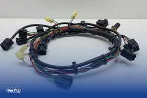
Would your car be able to run without wire harnesses? Not a chance. Wire harnesses connect all the electrical parts together. No harness means no
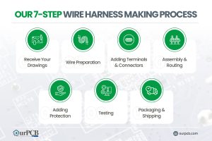
Making wire harnesses isn’t complicated. At OurPCB, we create custom wire harnesses for an expansive range of industries every day. While it’s a complicated process,

Prototype cable assemblies are the very important place in between PCB design ideas and interconnects. OurPCB brings prototype assemblies with PCB solutions to your tables.
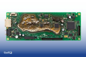
PCB thermal management prevents component overheating through strategic heat transfer techniques. Without proper thermal control, electronics are at risk of electronic failures through weakened solder
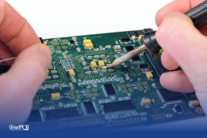
ContentsKey TakeawaysWhat is a Multilayer-Printed Circuit Board?How do Multilayer PCB Boards Work?Multilayer PCB ApplicationsMultilayer PCB Manufacturing Process: StepsMultilayer PCB Manufacturing MachinesBenefits of Multilayer Circuit BoardsWhat
We use cookies to improve your browsing experience, which may include personal information. By clicking "Agree," you accept our Privacy Policy and cookie use. You can change your cookie settings in your browser anytime.
Agree