


Flying probe testing uses 4 to 8 independent needles mounted on multi-axis robotic arms to contact pads, vias, and test points on PCBs without requiring a fixture.
Each probe has a positional accuracy of ±5 µm, and contacts are sequenced dynamically based on a CAD-derived test script.
The system can measure resistance, detect opens/shorts, verify component orientation (via diode/LED polarity), and validate net isolation up to 500 V.
Our flying probe systems support double-sided access and adaptive Z-axis compensation, making them ideal for prototypes, small batches, and low-volume Class III assemblies with BGA or fine-pitch components.

Boundary scan testing uses JTAG-compliant integrated circuits with built-in test registers to shift test data across pins without physical probing.
OurPCB configures boundary scan chains to test for missing pull-ups, bus contention, stuck-at faults, and inter-device connectivity.
This technique is essential for PCB assembly testing services involving BGAs, QFNs, and CSPs, where solder joints are optically and mechanically inaccessible.
Using tools like XJTAG or Corelis, our engineers run structural tests and functional vector scripts that monitor internal register responses, enabling deep digital path validation on complex, high-speed designs.

Automated optical inspection (AOI) scans every board using high-resolution cameras (up to 25 µm/pixel) to detect missing parts, incorrect polarity, lifted leads, tombstoning, and solder bridging.
Our inline AOI systems support 3D height profiling and compare actual assemblies against a golden reference using rule-based or neural-net criteria.
For dense, multilayer boards, X-ray inspection (AXI) uses 5 µm focal spot tubes to capture internal layers and verify hidden joint integrity under BGAs, LGAs, and stacked packages.
Both AOI and AXI are performed as part of OurPCB’s integrated PCB testing and inspection services, supporting IPC-A-610 Class III conformance and continuous yield monitoring.

High-potential and insulation resistance testing are performed using programmable dielectric testers capable of applying voltages from 100 V to 1500 VDC across isolated nets.
We verify insulation resistance up to 1000 MΩ and dielectric breakdown levels across creepage gaps, especially in high-voltage power PCBs or where double-insulated barriers are required.
This PCB testing service is essential for validating the safety of industrial control boards, battery management systems, and EV power converters.
OurPCB configures custom test setups with adjustable ramp rates, dwell time, and arc detection to meet IEC 61010 and UL standards for Class II/III applications.

![]()
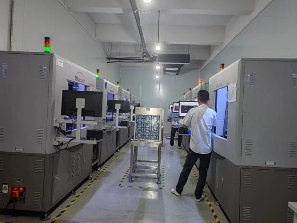
Factory-Ready for Ultra-Fine Assembly
Our dual 10,000 m² PCB assembly houses in Shenzhen and Shijiazhuang are equipped with high-speed SMT assembly lines capable of placing fine-pitch parts with ±25 µm tolerance.
Each line includes temperature- and humidity-controlled environments, active anti-static systems, and vacuum transport for handling thin or flex printed circuits.
![]()
Certified for High-Reliability Fine-Pitch Workflows
We are fully certified to ISO 9001, IATF 16949, and IPC-A-610 Class 2 & 3, supporting applications where fine-pitch PCB assembly must meet elevated acceptance criteria for solder joint geometry, lead coplanarity, and component body clearance.
Our QA workflows are built to handle fine-pitch PCBs requiring zero solder bridging and uniform joint fillets across dense arrays.
![]()
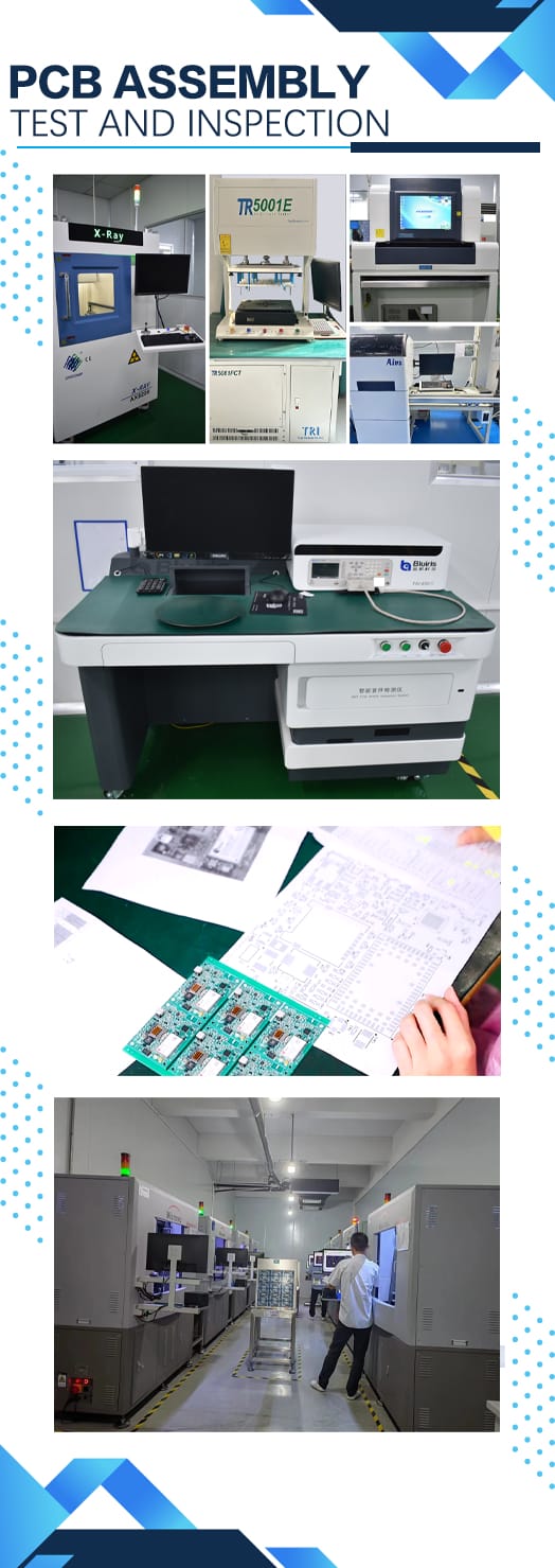
Multi-Platform Equipment with High Resolution
Our test infrastructure includes high-speed AOI (25 µm resolution), 5 µm X-ray inspection, 4-wire flying probe testers, and digital high-voltage dielectric testers.
Resistance measurements down to 10 mΩ, voltage capture from 100 mV to 1500 VDC, and insulation resistance over 1000 MΩ ensure detailed diagnostics for every PCB testing service.
Measurement integrity is maintained through ISO-calibrated instruments and logged reference values.
![]()
Full Traceability and Audit-Ready Reporting
We provide serialized test data with barcode traceability, linking each board to its BOM revision, test station ID, operator, and timestamp.
Reports include fail point coordinates, signal path diagnostics, image references (for AOI/AXI), and environmental test logs.
Our infrastructure supports full compliance with ISO 9001, IATF 16949, and medical-sector audit requirements, making our PCB functional testing services suitable for regulated deployments.
![]()
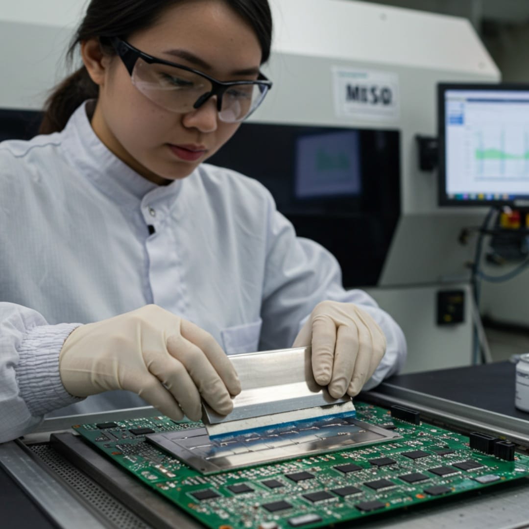
Class III Conformance with Reliability Testing
Our testing flows conform to IPC-A-610H Class III for high-reliability electronics, including burn-in testing, dielectric breakdown validation, and full visual and optical inspection of PCBs before final sign-off.
We support test plans that include ESS, startup sequence monitoring, and functional loop stress testing to simulate real-world deployment.
All solder joints, including BGA and QFN, are inspected using 3D AOI and void-mapped X-ray analysis.
![]()
48-Hour Quoting and Fixture Review
Comprehensive quotes for PCB testing services and fixture-based setups are delivered within 48 working hours.
For new PCBA designs, we provide a DFT assessment, pin map verification, and component access review before test planning begins.
This early-stage input improves test coverage, minimizes false failures, and enables rapid onboarding for customers requiring PCB assembly testing services with complex or high-mix builds.
Mon-Fri: 24 hours,
Sat: 9am-6pm, GMT+8
Reach us at
sales@ourpcb.net
24 hours online
+86-199-30589219
Mon-Fri: 24 hours,
Sat: 9am-6pm, GMT+8
Order options
Full test coverage for prototype and first-article assemblies.
Batch testing with AOI, X-ray, and ICT for Class II/III compliance.
Scaled test services with statistical process control and reporting.
★ What customers say
Easy to reach and proactive on status for our tested PCB assemblies.
Pricing on the tested PCB assemblies run was noticeably better than our previous supplier.
Careful packaging on the tested PCB assemblies and complete documentation.
The review team caught a stackup problem on our tested PCB assemblies early.
Our go-to for tested PCB assemblies now; repeat orders are always reliable.
Turnaround on our tested PCB assemblies order beat the quoted lead time by several days.

