PCB Reverse Engineering China
PCB reverse engineering is the process of analyzing and recreating circuit board designs. It involves extracting schematics, layouts, and component data from existing PCBs. OurPCB offers expert PCB reverse engineering services in China, helping clients recreate or improve circuit designs efficiently.


PCB Reverse Engineering China
PCB reverse engineering in China involves analyzing physical circuit boards to extract their design information. This process includes examining board layers, tracing connections, and identifying components. Skilled engineers use specialized tools and software to recreate accurate schematics and layouts.
China’s PCB reverse engineering industry has grown rapidly due to its strong electronics manufacturing base. Many companies, like OurPCB, offer advanced reverse engineering services. These firms combine technical expertise with cost-effective solutions, making China a global hub for PCB reverse engineering projects.
PCB Manufacturing Process


The Benefits of Partnering With OurPCB As Your China PCB Reverse Engineering Manufacturers?
OurPCB offers top-notch PCB reverse engineering services in China. Our team combines technical skills with industry experience to deliver accurate results. Here are the key benefits of choosing us:


- Highly skilled engineers with years of PCB analysis experience
- Continuous training in the latest reverse engineering techniques

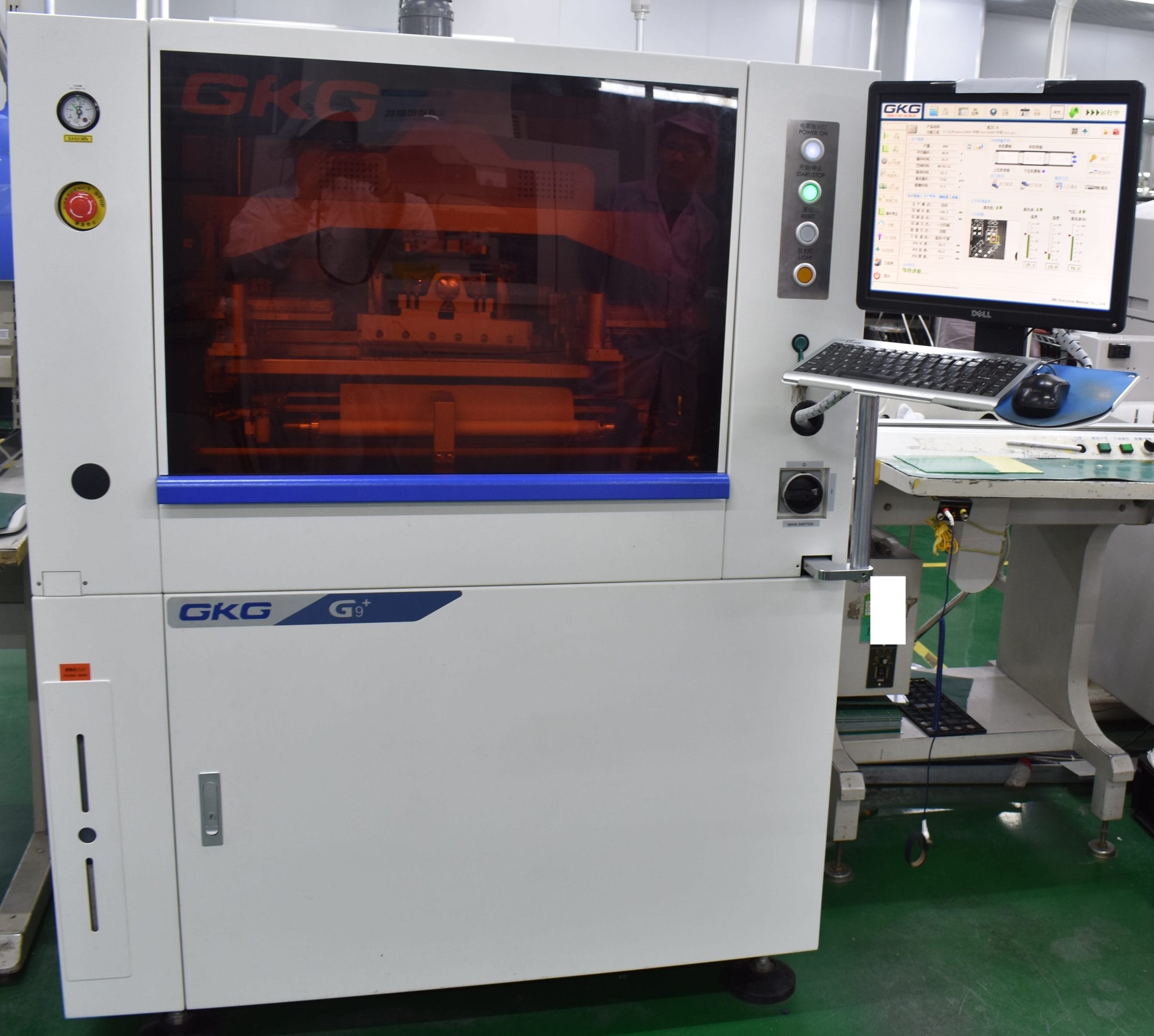
- State-of-the-art scanning and imaging equipment
- Cutting-edge software for precise schematic recreation

- Competitive pricing without compromising quality
- Flexible service options to fit various budget needs

- Efficient processes to deliver results faster
- Regular updates on project progress
Why Choose PCB Reverse Engineering Services, China?
PCB reverse engineering in China offers unique advantages for businesses worldwide. It combines technical expertise with cost-effective solutions. Here’s why China stands out:

- Access to the latest PCB analysis tools and software
- Cutting-edge facilities for accurate reverse engineering

- Lower labor costs translate to affordable services
- Bulk orders lead to significant cost savings

- Efficient processes speed up project completion
- Quick prototyping and testing capabilities

- Extensive knowledge in handling diverse PCB types
- Expertise in working with global electronics standards


PCB Assembly Services
OurPCB offers comprehensive PCB assembly services to complement our reverse engineering expertise. We ensure high-quality production of recreated or modified designs. Our services include:

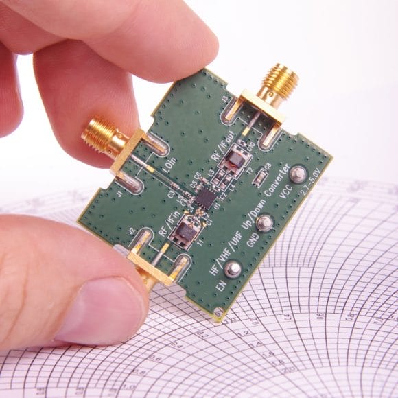
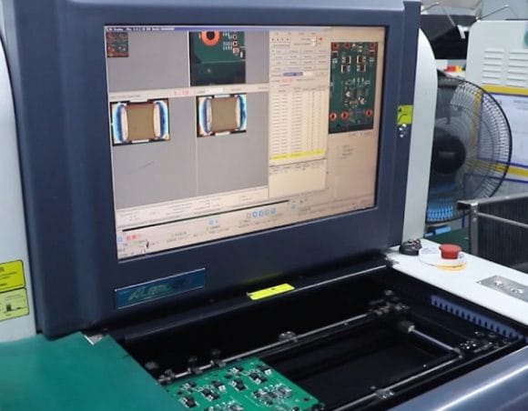
We use Surface Mount Technology for compact and high-performance PCB assembly. Our SMT process ensures precise component placement and soldering.

We offer flexible options for PCB assembly. We can work with your supplied components or provide full turnkey solutions, handling sourcing and assembly.

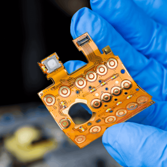
Our team delivers tailored assembly services to meet unique project needs. We adapt our processes to accommodate special designs or requirements.

We provide fast PCB assembly services without compromising quality. Our efficient processes ensure quick turnaround times for urgent projects.

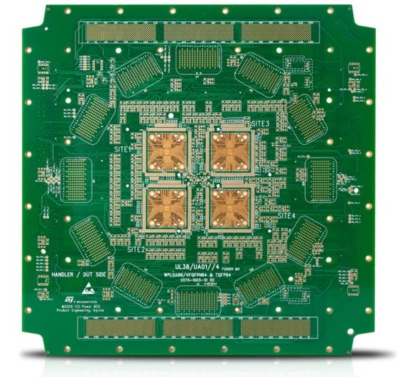
We adhere to strict IPC Class 3 standards for high-reliability PCB assembly. This service is ideal for aerospace, medical, and other critical applications.

We handle assembly for all types of IC packages. Our expertise covers BGAs, QFNs, CSPs, and other complex package types.
Millions of business and innovators use OurPCB


PCB Board Process
Order Received
- Component Procurement
- Preparation
- PCB Manufacture
- Make Process Flow
Soldering
- Solder Printing/Wave Soldering
- SMT/Plugging
- Inspection (repair if necessary)
- AOI (repair if necessary)
- Transfer
Parts Assembly
- Manual Assembly
- Cleaning
- Wire Screw
- Inspection
- Repair If Necessary
Finalization
- Final Confirmation
- Packing
- Shiping
Technical Capabilities
OurPCB boasts advanced technical capabilities for PCB reverse engineering. We use high-resolution X-ray systems and 3D scanning technology for detailed board analysis. Our software suite includes industry-standard tools for schematic capture and PCB layout recreation. We can handle boards up to 50 layers and work with various PCB materials. Our team is skilled in decoding complex circuits and identifying obsolete components.


Capabilities & Services
- PCB Layout Design
- Up to 50 Layers
- 0.3mm BGA Pin Spacing
- 60GHz High Frequencies
- Stack-up Design
- Rigid, Flex, HDI, High-speed, Power Boards
- 100,000+ PIN
- 2.4mil Trace Width/Spacing
- Controlled Impedance
- DFM Check


Mon-Fri: 24 hours,
Sat: 9am-6pm, GMT+8

Reach us at
[email protected]
24 hours online

+86-199-30589219
Mon-Fri: 24 hours,
Sat: 9am-6pm, GMT+8
Reverse Engineering PCB China FAQs
Can you make a PCB clone that is 100% the same as the original board?
A PCB copy can replicate an original PCB design, using engineering files. However, slight variations can occur during PCB manufacturing, despite using precise Gerber file inputs. The PCB board may differ slightly from the original PCB due to production limitations. Multilayer and PCB module specifics can affect PCB production accuracy.
If reverse engineering is not precisely cloning the original design, what is it for?
The reverse engineering process uncovers the PCB schematic diagram, BOM list, and design. It helps understand the original PCB functionality for future PCB design improvements. It also enables IC unlock to modify or improve the electronic product. Reverse engineering allows accurate replication of similar or new board designs.
Is a PCB sample re-usable?
A physical PCB sample is typically not reusable due to potential wear during PCB service. However, the PCB file or Gerber file can be reused for PCB production. In some cases, a multilayer PCB may be reworked or modified for use. Engineering files are crucial for evaluating the reusability of a PCB board.