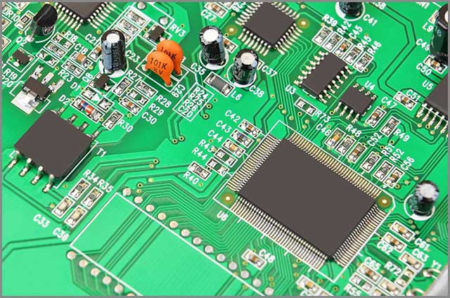
Printed Circuit Boards (PCBs) form the backbone of most modern electronics, allowing for efficient electrical connections between components. The choice of PCB material can significantly impact the performance, durability, and overall cost of a project. From consumer electronics to aerospace, selecting the right material is crucial to ensure that your circuit board functions as intended under various conditions. In this blog, we’ll explore the different types of PCB materials, their properties, and where they are best applied.
Contents
- What is PCB Material?
- Key Properties to Consider in PCB Materials
- Common Types of PCB Materials
- Specialty PCB Materials
- Ceramic-Based PCBs
- Rogers Materials
- What are the different grades of PCB materials and their characteristics?
- PCB Material Selection Guide
- Quality Considerations
- Cost Considerations
- Power and Heat Considerations
- PCB Substrate Materials – What Type is Right for Your PCB?
- 1.Copper Foil Requirements
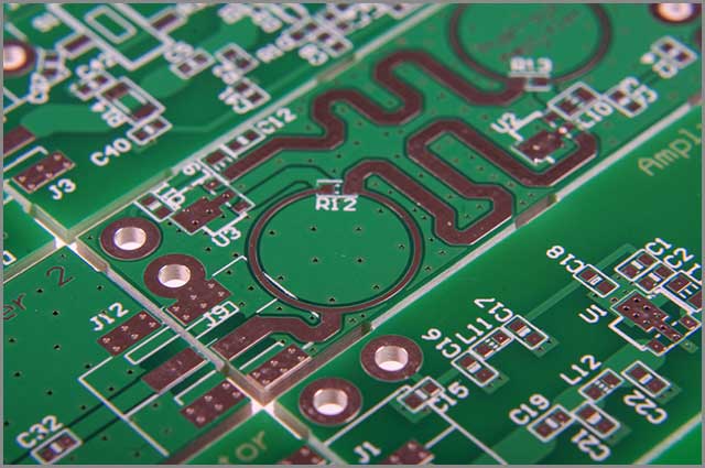
- 2.Insulating Dielectric Laminates
- 3.Why High Speed and High Frequency Are Important for Your PCB
- Types of Substrate Materials usable in High-Frequency PCBs?
- 4.Thermal Requirements of PCBs
- How to Choose PCB Substrate Materials
What is PCB Material?
PCB material refers to the substrate and laminate used to build the physical structure of the circuit board. These materials act as the foundation of the PCB, providing insulation between the conductive copper layers and helping manage the thermal and mechanical stresses the board might experience. Choosing the correct material directly influences the PCB's ability to perform reliably across a wide range of conditions, such as temperature variations, mechanical stresses, and electrical demands.
Key Properties to Consider in PCB Materials
When selecting a PCB material, several key properties come into play, affecting both performance and cost:
- Electrical Properties: Dielectric constant (Dk) and dissipation factor (Df) determine how well the material supports signal transmission, especially at high frequencies.
- Thermal Properties: The glass transition temperature (Tg) and thermal conductivity measure how well the material can withstand heat and manage dissipation.
- Mechanical Properties: Flexural strength, tensile strength, and the material’s ability to handle vibrations without damage.
- Cost Considerations: High-performance materials often come with a higher price tag, so it’s important to balance material properties with the project budget.
Special Offer: Get $100 off your order!
Email [email protected] to get started!
Common Types of PCB Materials
Different PCB materials are available, each with its unique set of characteristics suited for specific applications. Below is a breakdown of the most commonly used PCB materials:
| PCB Material | Composition | Characteristics | Applications |
|---|---|---|---|
| FR-4 (Flame Retardant 4) | Woven fiberglass and epoxy resin | - Most widely used - Flame resistant - Good electrical insulation |
Consumer electronics, general electronics |
| Polyimide | Flexible plastic material | - Excellent thermal stability - High heat resistance |
Aerospace, automotive, flexible PCBs |
| PTFE (Polytetrafluoroethylene) | Teflon-based material | - Low signal loss - Superior high-frequency performance |
RF and microwave circuits |
| Metal-Core (Aluminum/Copper) | Metal core with dielectric layer | - Enhanced heat dissipation - High rigidity |
Power electronics, LED lighting |
| Rogers Materials | Thermoset and thermoplastic laminates | - Superior dielectric properties - Stable at high frequencies |
Telecommunications, high-speed applications |
Each of these materials serves distinct purposes based on their thermal, mechanical, and electrical properties.
Specialty PCB Materials
In addition to common PCB materials, specialty materials are used for more demanding applications. These materials are often chosen for their ability to withstand extreme conditions, both in terms of temperature and performance.
Ceramic-Based PCBs
Ceramic-based PCBs use ceramic materials like alumina and aluminum nitride, which offer excellent thermal conductivity and electrical insulation. They are ideal for high-power devices and military applications that require robust materials capable of dissipating heat without warping or losing electrical performance. Applications: High-power electronics, aerospace, and military technology.
Rogers Materials
Rogers materials are known for their superior dielectric properties, making them suitable for high-frequency circuits. They are thermoset and thermoplastic laminates that offer stability under high-frequency conditions, which makes them highly desirable in telecommunication and data transfer industries. Applications: Telecommunications, high-speed data transfer circuits.
What are the different grades of PCB materials and their characteristics?
PCB materials are classified into various grades based on their performance characteristics, each suited for specific applications. The following table summarizes the four main grades of PCB materials, their key features, and examples:
| Grade | Key Characteristics | Typical Applications | Example Material |
|---|---|---|---|
| Standard Grade |
|
Consumer electronics, industrial equipment | FR-4 |
| High-Speed Grade |
|
Telecommunications, high-speed digital circuits, RF applications | Rogers RO4350B |
| High-Temperature Grade |
|
Automotive, aerospace, military applications | Polyimide-based materials |
| Halogen-Free Grade |
|
Green electronics, medical devices | Isola IS410 |
PCB Material Selection Guide
Quality Considerations
Quality consideration is paramount when selecting PCB materials. Regardless of where your PCB will serve, the documents must have to meet the intended requirements. The board shouldn’t quickly fail due to physical stress. You will not compromise the original PCB's fundamental parts with durable PCB materials, especially when undertaking hardware updates.
Cost Considerations
The cost of PCB materials matters a lot. Many designers use either gold or solder tabs. However, gold tabs are a little bit expensive. When it comes to buried and blind vias, buried vias tend to be cheaper. Lastly, considering line and width spacing either above or below six mils, spacing above six mils does incur higher costs.
Power and Heat Considerations
Power and heat are some of the most critical factors determining the reliability and usefulness of a PCB prototype. To be on the safe side, ensure that you check for your chosen board’s thermal capacities.
PCB Substrate Materials – What Type is Right for Your PCB?
The materials that you select for your PCB will have an impact on the functionality of your product. Going for the best PCB substrate materials can broadly impact durability, performance, and plenty of other board features. Here is how to go about selecting the best materials for your board.
1.Copper Foil Requirements
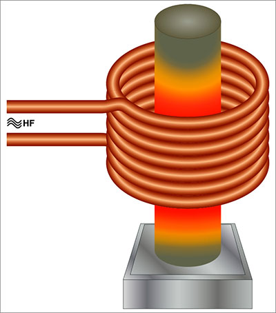
Have you ever come across the term HDI PCB? If not, then it means High-Density Interconnect Printed Circuit Board. PCBs require copper foils for practical functionality. A copper foil is a harmful electrolytic material that you can find on the circuit's base layer. The copper foil acts as the conductor of a printed circuit board.
How Surface Roughness Can Affect the Quality of Your PCB
If you want to have a proper PCB, you must consider matters to do with the copper foil surface's roughness. Roughing ensures that the conductors have peel strength and that the copper foil's bonding and the substrate material is optimal. Nowadays, the standard roughness stands at around 5μm. To boost the peel strength, you may have to embed a hump on the foil into the substrate to ensure that the severity stays as low as possible.
2.Insulating Dielectric Laminates
The buildup process is an essential property of HDI PCBs. In case you resort to using resin-coated copper or use a combination of copper foil lamination and prepreg cloth of epoxy glass, you may design a beautiful circuit. Today, manufacturers implement SAP and MSPA technologies. Such has brought about a generation of copper conduction planes by applying chemical copper plating with insulating dielectric film lamination. The thin copper plane is the main reason why manufacturers can produce beautiful circuits.
Why Lamination Dielectric Material Is Crucial for SAP
If you are going to design HDI PCBs, then you need to factor in lamination materials and its requirements. You need to factor in include thermal capacity, dielectric performance, bonding, and insulation. In multi-layer PCBs, the substrate materials should be in a position to help in the reduction of thermal expansion coefficient in addition to dielectric property while at the same time, securing optimal resistance to heat. These properties make the right choice of substrate material since they can achieve the entire performance goals at an acceptable cost. When the space and width of circuits are below 10μm, there’s no option but to use SAP technology when manufacturing them. In large scale production, MSPA technology comes in to use thin copper foil to insulate dielectric lamination.
3.Why High Speed and High Frequency Are Important for Your PCB
Technology continues to evolve every day, with innovations such as wireless connections, high frequencies, and high speeds being apt examples of the latest technological innovations. High-speed designs are the topic of almost every expert in the industry. There’s a possibility of making a difference between: Medium Dk/Df laminate PCBs have Df that’s no higher than 0.010, and Dk of a maximum of 4. Low Dk/Df laminate PCBs – have a Df of less than 0.005 with a Dk of not more than 3.7.
Types of Substrate Materials usable in High-Frequency PCBs?
You can find the best materials to use in one of the following:
- Fluorine-series-resin – materials such as PTFE consist of the best dielectric performance and a great choice, especially if you require at least 5GHz frequency. While they are a bit costly, they are the best since they have a high thermal expansion coefficient.
- PPE and PPO resin – it’s a suitable option for 1-10GHz frequencies. These secure an excellent all-round performance of your PCB, ensuring that factors like heat and contaminants do not destroy PCB functionality.
- Modified epoxy resin – these are an excellent choice for frequencies between 1GHz and 10GHz. Generally, they are affordable and a reason as to why they are so popular.
4.Thermal Requirements of PCBs
As a component carrier, a PCB is the main component aimed at achieving coherent thermal management. In advance, designers have to factor in the following primary thermal considerations:
- Available space and mounting peripherals
- The amount of heat and power loss
- How to conduct heat to the radiator
- Heat sources on the PCB
- Reliability requirements, such as cycle stability
- Application temperatures and ambient temperatures
What Would Material Be the Best Choice for Heat Conductivity?
When you want to combine excellent heat conductivity, optimal cost, and availability, the material must be aluminum. While aluminum tends to be cheap, it can also bring about an excellent electrical connection while ensuring that everything is soldered with lead free solder.
How to Choose PCB Substrate Materials
There are three different PCB choices that you can pick; rigid, flexible, or flex-rigid PCBs. The goal is to choose a board that will be perfect for your product. Many people go for compact shape and size, though they forget about performance. Polyimide is a smart choice since it’s versatile and can fit into different categories, such as black, transparent, and white.
Additionally, it ensures that there’s a low thermal expansion coefficient and, at the same time, maintains adequate resistance to matters concerning heat. Mylar substrate tends to be highly elastic in addition to having excellent resistance to several environmental factors.
Additionally, it’s relatively affordable, a reason as to why a majority of users use it. For flexible boards, polytetrafluoroethylene and advanced polyimide substrate are the best type of material to use—flexible PCB used in many industries, such as smartphones, gadgets, and the medical industry.
Back to top: PCB Materials
Special Offer: Get $100 off your order!
Email [email protected] to get started!