Contents
- What is a High-Speed PCB Design?
- Key Components of High-Speed PCB Design
- Applications of High-Speed Circuit Boards
- High-Speed PCB Design Guidelines
- Reference Planes and Return Paths
- Board Stackup Design
- Controlled Impedance Traces
- Signal Integrity Management
- Trace Length and Routing
- Differential Pair Routing
- Power Distribution Network (PDN) Design
- Fundamentals
- Decoupling Strategy
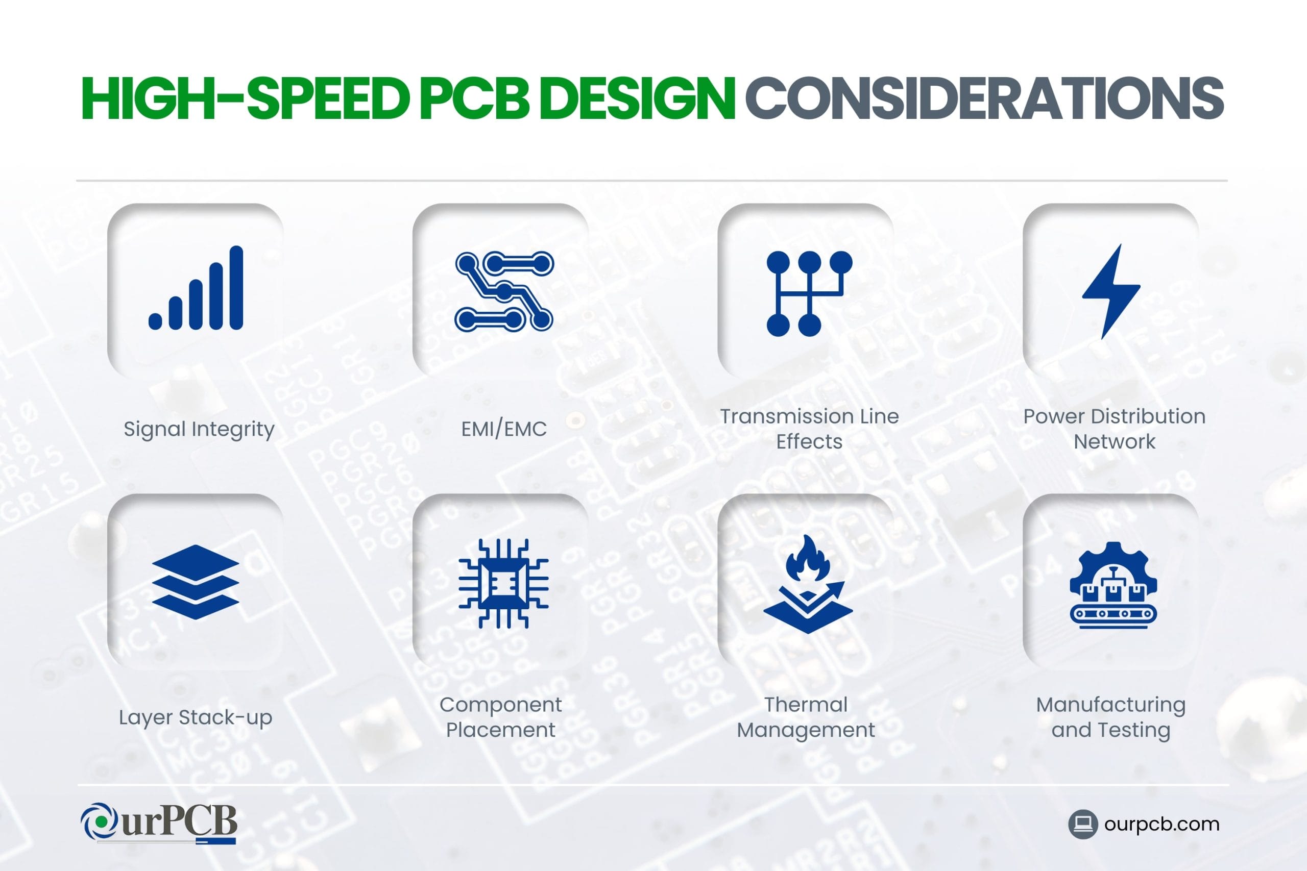
- High-Speed PCB Design Considerations
- EMI/EMC Control
- Thermal Management
- Material Selection
- Component Placement
- Manufacturing and Testing
- When to Use High-Speed Design
- High-Speed Interfaces
- Electrical Length Considerations
- Wireless Interfaces
- OurPCB Manufacturing Services
- FAQs
- What is considered a high-speed circuit?
- What's the difference between high-speed and low-speed signals?
- What are the top three important steps in PCB design?
- What controlled impedance tolerances can OurPCB maintain?
- How do I specify controlled impedance requirements?
What is a High-Speed PCB Design?

High-speed PCB design creates circuit boards that handle high-frequency signals and fast digital transitions. When signal rise times are below 1 nanosecond or frequencies exceed 50-100 MHz, interconnects behave as transmission lines where signal wavelengths compare to trace lengths.
In this regime, the traditional point-to-point connection model fails, requiring engineers to account for complex electromagnetic effects. High-speed PCB design focuses on maintaining signal integrity, controlling impedance, minimizing EMI, and managing power delivery.
Key Components of High-Speed PCB Design
Our comprehensive signal integrity PCB solutions include these essential elements:
- Controlled Impedance Transmission Lines: Precisely designed traces that maintain consistent impedance throughout the signal path
- Strategic Reference Planes: Carefully designed ground and power planes providing low-impedance return paths
- Advanced Stackup Design: Optimized layer arrangements controlling impedance, crosstalk, and power distribution
- Signal Integrity Management: Techniques preserving signal quality by controlling reflections, crosstalk, and timing issues
- Power Integrity Engineering: Methods ensuring clean, stable power delivery through proper PDN design
- EMI/EMC Control: Strategies minimizing electromagnetic interference and ensuring compatibility
Applications of High-Speed Circuit Boards
- High-Performance Computing: Servers with multi-gigahertz processors and high-bandwidth memory interfaces requiring precise timing
- Telecommunications Equipment: Network infrastructure handling 10-400 Gbps data rates
- Advanced Networking Devices: Equipment implementing 10G/25G/100G Ethernet standards
- High-Definition Video Systems: Digital video equipment processing 4K/8K signals
- Radar and RF Applications: Systems operating at microwave frequencies
High-Speed PCB Design Guidelines
Reference Planes and Return Paths
- Maintain continuous ground and power planes for low-impedance return paths
- Keep signal layers adjacent to reference planes for controlled impedance
- Avoid splitting reference planes under high-speed traces to prevent up to 50% signal reflection
- Place stitching capacitors and vias near unavoidable plane transitions
Board Stackup Design
- Design stackups with alternating signal and plane layers to ensure reference planes for all signal layers
- Use symmetrical stackups to prevent manufacturing warpage
- Select appropriate high-frequency materials; high-performance materials like Rogers RO4350B offer Df values of 0.005-0.01, reducing signal loss by 30-50% at multi-GHz frequencies
- Consider dielectric constant stability across frequency and temperature
Example 8-Layer High-Speed PCB Stackup:
| Layer | Type | Material | Thickness | Function |
|---|---|---|---|---|
| 1 | Signal | Copper | 1 oz | High-speed signals |
| Dielectric | FR-4 | 4 mil | ||
| 2 | Plane | Copper | 1 oz | Ground reference |
| Dielectric | FR-4 | 4 mil | ||
| 3 | Signal | Copper | 0.5 oz | High-speed signals |
| Dielectric | FR-4 | 4 mil | ||
| 4 | Plane | Copper | 1 oz | Power |
| Core | FR-4 | 40 mil | ||
| 5 | Plane | Copper | 1 oz | Ground reference |
| Dielectric | FR-4 | 4 mil | ||
| 6 | Signal | Copper | 0.5 oz | High-speed signals |
| Dielectric | FR-4 | 4 mil | ||
| 7 | Plane | Copper | 1 oz | Ground reference |
| Dielectric | FR-4 | 4 mil | ||
| 8 | Signal | Copper | 1 oz | High-speed signals |
Controlled Impedance Traces
- Control trace width and spacing to achieve target impedance values
- For a typical 50Ω microstrip on FR-4 (Dk ≈ 4.2) with 1 oz copper and H = 4 mil, trace width is approximately 7-8 mil
- Use impedance calculators or field solvers for accurate calculations: Z₀ ≈ (87/√(Dk + 1.41)) × ln(5.98H/(0.8W + T))
- Specify impedance requirements clearly in design documentation with target values, tolerances, and designated nets
Signal Integrity Management
Reflections and Termination
- Maintain consistent impedance throughout signal paths
- Implement appropriate termination:
- Series termination: Resistor near the driver (33-50Ω)
- Parallel termination: Resistor at the receiver (50-100Ω)
- Thevenin termination: Voltage divider network establishing impedance and DC bias
- Pay special attention to vias, connectors, and component pads as impedance discontinuity sources
Crosstalk Management
- Follow the 3W spacing rule for parallel traces (spacing ≥ 3× trace width) to reduce crosstalk below 5%
- Increase spacing for sensitive signals or fast edge rates to 5W or greater
- Use guard traces between critical signals
- Implement orthogonal routing between adjacent layers
Trace Length and Routing
- Keep high-speed traces short; above 1 GHz, each additional inch adds 150-180 ps delay and 0.5-1.0 dB attenuation
- Implement length matching; DDR4 typically requires matching within ±25 mils (0.635mm)
- For serpentine patterns:
- Use gentle turns (45° or curved)
- Maintain at least 3W spacing between segments
- Avoid resonant structures (¼ wavelength segments)
- Use 45° bends instead of 90° for improved manufacturing and reduced impedance effects
Differential Pair Routing
- Route pairs with tight coupling (spacing ≈ trace width) for noise rejection
- Maintain consistent spacing throughout to preserve differential impedance
- Match trace lengths within 5 mils (0.127mm) to prevent skew
- Keep differential pairs on the same layer when possible
- Maintain appropriate impedance per interface:
- USB: 90Ω differential
- HDMI/DisplayPort, PCIe, SATA, Ethernet: 100Ω differential
Special Offer: Get $100 off your order!
Email [email protected] to get started!
Power Distribution Network (PDN) Design
Fundamentals
- Maintain low impedance (<0.1Ω) between power and ground at all frequencies
- Calculate target impedance: Z_target = V_ripple / I_transient (typically 5% of supply voltage)
- PDN components include power/ground planes, bulk capacitors (low frequency), decoupling capacitors (mid frequency), and on-die capacitance (high frequency)
Decoupling Strategy
- Implement multi-tiered approach:
- Small capacitors (0.01-0.1μF) near IC power pins
- Medium capacitors (1-10μF) near component groups
- Bulk capacitors (47-100μF) near power entry points
- Select values addressing the full frequency spectrum based on self-resonant frequencies
- Use multiple smaller capacitors in parallel to reduce inductance
- Place vias directly at capacitor pads to minimize connection path
High-Speed PCB Design Considerations

EMI/EMC Control
- Implement proper grounding with solid planes, short return paths, and ground fills
- Use appropriate shielding: board-level cans, sandwich structures, and edge treatments
- Control edge rates to reduce high-frequency energy when timing allows
Thermal Management
- Account for thermal effects on signal integrity:
- Increased conductor resistance
- Dielectric constant variations
- Component parameter drift
- Implement appropriate cooling through copper pours, thermal vias, and strategic airflow
Material Selection
| Material Type | Dk Range | Df Range | Suitable For |
|---|---|---|---|
| Standard FR-4 | 4.0-4.5 | 0.017-0.025 | Up to 3 GHz |
| Mid-loss FR-4 | 3.8-4.2 | 0.010-0.015 | Up to 5-8 GHz |
| High-speed FR-4 | 3.5-4.0 | 0.005-0.010 | Up to 10 GHz |
| Rogers RO4350B | 3.48 | 0.0037 | Up to 20+ GHz |
| Rogers RT/duroid | 2.2-10.2 | 0.0009-0.0022 | Up to 40+ GHz |
- Consider cost vs. performance; high-performance materials cost 5-10x more but may only be needed for critical signals
Component Placement
- Place components strategically to minimize trace lengths
- Group related components for improved signal integrity:
- Keep memory devices close to controllers
- Position differential pair components for direct routing
- Separate analog and digital sections
Manufacturing and Testing
- Design for manufacturability with appropriate specifications
- Include test points and impedance test structures
- Specify TDR testing for critical traces
When to Use High-Speed Design
High-Speed Interfaces
| Interface | Data Rate | Typical Impedance | Rise Time |
|---|---|---|---|
| PCIe Gen3 | 8 GT/s | 100Ω diff | <100 ps |
| PCIe Gen4 | 16 GT/s | 100Ω diff | <50 ps |
| DDR4 | 3200 MT/s | 40-50Ω single-ended | <150 ps |
| USB 3.0 | 5 Gbps | 90Ω diff | <100 ps |
| HDMI 2.0 | 6 Gbps | 100Ω diff | <100 ps |
| 10G Ethernet | 10 Gbps | 100Ω diff | <50 ps |
Electrical Length Considerations
- Apply high-speed techniques when trace length exceeds critical length:
- Trace Length > (tr × c) / (2 × √εr)
- Example: with 100ps rise time on FR-4 (εr ≈ 4.2), critical length ≈ 7.3 mm
Wireless Interfaces
- Required for RF functionality with on-board antennas (typically 50Ω traces)
- Necessary for RF connectors (SMA, U.FL, MMCX)
- Generally beneficial above 100 MHz, critical above 1 GHz
OurPCB Manufacturing Services
OurPCB offers specialized manufacturing for high-speed PCBs:
- Precise material selection with verified Dk/Df properties
- Controlled etching processes (±1 mil tolerance)
- Multi-point TDR testing
- Advanced layer alignment
- Specialized surface finishes for high-frequency performance
Our team offers design optimization, pre-manufacturing reviews, and impedance simulation to identify potential issues before fabrication.
FAQs
What is considered a high-speed circuit?
A circuit with frequencies above 50-100 MHz or rise times below 1 nanosecond, or where trace length makes the interconnect "electrically long" compared to signal rise time.
What's the difference between high-speed and low-speed signals?
| Characteristic | Low-Speed Signals | High-Speed Signals |
|---|---|---|
| Signal Path | Simple point-to-point connections | Transmission lines requiring impedance control |
| Signal Reflections | Negligible | Significant without proper termination |
| Crosstalk | Minimal | Potentially severe requiring spacing control |
| Return Path | Any convenient ground | Must follow path directly beneath signal |
| Timing | Less critical | Precisely controlled for skew and jitter |
What are the top three important steps in PCB design?
- Proper stackup design: Optimal layer arrangement with controlled dielectric thicknesses and strategic plane placement
- Strategic component placement: Positioning to minimize trace lengths and enable optimal routing
- Controlled impedance routing: Implementing precise geometries and maintaining consistent reference planes
What controlled impedance tolerances can OurPCB maintain?
We maintain ±10% tolerances through our standard processes, with ±7% possible for critical applications. Our process includes pre-manufacturing simulation, precise material selection, controlled etching, and TDR testing.
How do I specify controlled impedance requirements?
Include the following specifications:
- Target impedance values for each transmission line type
- Layer locations of controlled impedance traces
- Acceptable tolerance (typically ±10%)
- Critical nets requiring control
- Test point locations for verification
Mark your order with "Controlled Impedance Required" and reference any impedance calculations performed.
Back to Top: High-Speed PCB Design: Essential Guidelines and Advanced Techniques
Special Offer: Get $100 off your order!
Email [email protected] to get started!