- PCB Manufacturer
- PCB Assembly
- Fine Pitch
Fine Pitch PCB Assembly for High-Density, High-Precision Electronics
We provide fine-pitch PCB assembly services for applications where controlled impedance, thermal management, and compact layouts are mandatory.
These assemblies are used in high-density PCB designs where the number of electronic components per unit square area exceeds standard SMT density and requires tighter tolerances, enhanced solder control, and sub-25 µm placement precision.
Our team reviews PCB fabrication tolerances, stencil aperture design, and ball pitch requirements to optimize every pitch PCB assembly for long-term reliability.
✅ Fine pitch PCB assembly support down to 8 mil (0.2 mm).
✅ SMT assembly lines with ±25 µm accuracy for high pin count and chip scale packages.
✅ ISO 9001, IATF 16949, and IPC-A-610 Class 2 & 3 certified for electronic assembly.


PCB Manufacturing Process


Why Choose OurPCB for Your EV Charger PCBs?
Choosing the right PCB manufacturer for EV chargers means more than just hitting specifications; it’s about consistent quality, fast lead times, and a partner who understands the regulatory and reliability pressures of electric vehicle infrastructure. OurPCB delivers that foundation across every layer of design and production.


OurPCB operates two fully equipped manufacturing sites in China, each covering over 10,000 square meters of production space.
These facilities are built to support high-volume EV charger PCB assembly across SMT, THT, and hybrid processes. Both sites are vertically integrated, allowing for seamless control over fabrication, assembly, testing, and final packaging.
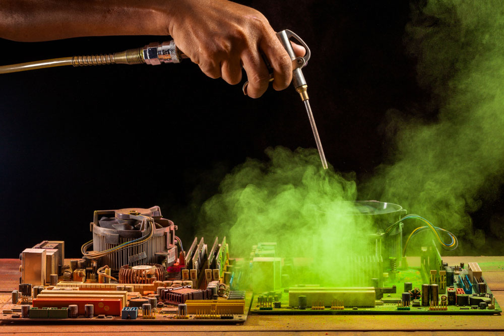
Production lines are outfitted with advanced equipment, including solder paste printers, reflow ovens, AOI systems, BGA rework stations, and ICT testers. Dedicated zones are maintained for nitrogen reflow, X-ray inspection, and conformal coating to support high-voltage PCB applications in EV charging systems.

OurPCB manufactures EV charger PCBs in facilities certified to ISO 9001:2015 and IATF 16949:2016, meeting the requirements for automotive and high-reliability electronics.
We build to IPC-A-610 Class 2 by default, with full capability for Class 3 when higher durability or safety margins are required.
Our engineering workflows also support PCB assembly projects targeting IEC 61851 and ISO 15118, a smart charging protocol enabling EV authentication via the control pilot line.

Since 2007, OurPCB has delivered precision PCB assembly services to over 3,000 customers across 40 countries.
Our client base spans electric vehicle manufacturers, automotive Tier 1 suppliers, charging infrastructure developers, and industrial energy OEMs. This depth of experience enables us to meet the performance, cost, and compliance expectations of global EV programs.
We support both prototype and mass production needs, with structured NPI workflows and repeatable process controls.
Clients rely on our technical stability, fast response times, and consistent output across multilayer charger boards, control PCBs, and power regulation modules.

OurPCB provides full engineering support to streamline EV charger PCB design and accelerate production readiness.
Our in-house team reviews all Gerber files, BOMs, and stack-ups for manufacturability, focusing on high-voltage isolation, trace current capacity, and controlled impedance requirements.
We assist with impedance matching, conductor width calculations, and interlayer clearance analysis to meet the demands of AC and DC charger designs.
For complex builds, we offer design feedback for structures, thermal reliefs, and pad geometries, along with guidance on compliance with IPC, IEC, and regional safety standards.

OurPCB sources all components for EV charger PCB assemblies from authorized global distributors, including Mouser, Digi-Key, Future Electronics, and WPG.
We manage lifecycle status, lead time risk, and cross-referencing to ensure stable sourcing for automotive-grade components such as SiC MOSFETs, gate drivers, current sensors, and power supply ICs.
All incoming materials are subject to ESD-safe handling, lot-level inspection, and barcode tracking throughout the assembly process.

OurPCB supports rapid program timelines with fast and accurate quoting for EV charger PCB builds.
Standard quotes for bare PCB fabrication are delivered within 8 working hours, while full turnkey PCBA quotes with component sourcing are provided within 48 hours.
Our staff works directly with engineers and procurement teams to resolve DFM questions, confirm delivery schedules, and manage revisions across global time zones.
Why Choose OurPCB for Fine-Pitch PCB Assembly?
OurPCB specializes in fine pitch PCB assembly for complex, miniaturized systems that require sub-0.5 mm pitch spacing, hidden interconnects, and precision solder control. With over 20 years of experience in PCB manufacturing and assembly, we support fine-pitch projects through every stage, from layout review to final assembly and production, using calibrated automation, Class III standards, and verified traceability systems.

Our dual 10,000 m² PCB assembly houses in Shenzhen and Shijiazhuang are equipped with high-speed SMT assembly lines capable of placing fine-pitch parts with ±25 µm tolerance.
Each line includes temperature- and humidity-controlled environments, active anti-static systems, and vacuum transport for handling thin or flex printed circuits.

We are fully certified to ISO 9001, IATF 16949, and IPC-A-610 Class 2 & 3, supporting applications where fine-pitch PCB assembly must meet elevated acceptance criteria for solder joint geometry, lead coplanarity, and component body clearance.
Our QA workflows are built to handle fine-pitch PCBs requiring zero solder bridging and uniform joint fillets across dense arrays.

All assemblies involving ball pitch under 0.5 mm, QFN, or PoP packages undergo X-ray inspection, SPI, and AOI with 15 µm resolution optics.
We detect voids, open leads, insufficient solder, lifted terminations, and hidden shorts. This inspection process is a requirement for successful assembly when working with components that provide no visible solder access.

Every fine-pitch electronic assembly receives a DFM and DFA review focused on stencil coverage, aperture tuning, pcb design limitations, and routing near fine-pitch ICs.
We assist in verifying pad design, thermal pad exposure, and via escape planning, important for high I/O packages like BGA and chip scale layouts where misalignment or solder blockage can compromise yield.

We offer full assembly component sourcing through partners like Digi-Key, Mouser, and WPG, including traceable lots for hard-to-find or moisture-sensitive electronic components.
Components are stored under MSL-compliant conditions, with drying cabinets and vacuum packaging for all incoming fine-pitch parts.


How do We Clean No-Clean Flux and Prepare for Conformal Coating?
At OurPCB, we remove no-clean flux during the PCBA cleaning process to prevent insulation resistance loss, support coating adhesion, and avoid inspection rejection in Class 2 and 3 assemblies.
Although low-solid no-clean flux is engineered to remain on the board, its residue absorbs moisture, lowers surface resistivity, and disrupts conformal coating uniformity, especially near component edges or mask-defined pads.
Our PCBA cleaning procedures are based on flux type, component density, and coating thickness requirements, and are qualified using ionic cleanliness testing, white residue detection, and surface preparation metrics that ensure coating and inspection compliance.
Why We Remove No-Clean Flux
We remove no-clean flux residue because its remaining solids form hygroscopic films with ionic content capable of enabling leakage currents under bias. These residues often contain halide activators or rosin derivatives that, in humid environments, allow ionic mobility as low as 10⁸ Ω insulation resistance across narrow conductor spacing.
On high-density printed circuit board assemblies, especially those with ≤0.3 mm pitch, this can lead to dendritic growth, moisture-induced tracking, and eventual open or short failures. In Class 3 applications, even visually benign residues violate IPC J-STD-001 Section 8.3.1, prohibiting any visible residue under conformal coating.
Removing these residues is required to maintain dielectric performance and prevent latent field degradation.
How We Remove No-Clean Flux
Our cleaning strategy depends on the flux chemistry and board design. For fully assembled SMT boards, we use vapor degreasing with HFE-72DA or Vertrel XF, which condense at 55 °C – 65 °C onto the PCBA surface, dissolve polar and non-polar residues, and evaporate without leaving water or exposing components to immersion.
In rework areas or where selective cleaning is required, we use Decotron T383 or high-purity IPA with aerosol precision nozzles to rinse solder ball traps and low-solids residue from around pads.
The process is followed by 30 psi filtered air drying or vacuum-assisted drying to prevent water adsorption beneath packages. Surface prep is validated using surface insulation resistance (SIR) measurements, ionic testing (<1.56 µg/cm² NaCl equivalent), and UV light to detect fluorescence from missed residues.
How this Enables Coating and Inspection
Removing flux residue allows for consistent conformal coating flow and edge adhesion, especially in boards using urethane or acrylic coatings. Cleaned surfaces increase surface energy, improving film wetting and eliminating common defects like dewetting, bridging, or edge lift.
Coating adhesion strength improves from 1.2 N/mm (on flux-contaminated surfaces) to over 2.5 N/mm on properly cleaned copper and solder mask regions, reducing delamination risk during thermal cycling. In addition, a clean PCB surface ensures that automated optical inspection (AOI), UV inspection, or manual visual checks can accurately detect voids, bubbles, or skipped areas.
For applications in automotive ECUs, implantable medical devices, or high-speed digital RF systems, surface cleanliness before coating directly correlates to long-term device reliability in harsh conditions.


Our Fine Pitch PCB Assembly Capabilities
OurPCB provides fine pitch PCB assembly services for advanced electronic systems requiring component pitches down to 8 mil. Every fine-pitch circuit board is evaluated against strict PCB fabrication tolerances, with DFM input provided before production to reduce defects and improve yield.
We manufacture fine-pitch PCB assembly for components with center-to-center spacing as low as 0.3 mm (12 mil) and down to 8 mil for reviewed designs.
Our pick and place machines operate at ±25 µm placement tolerance with real-time optical correction, supporting the exacting alignment needed for fine-pitch parts like BGA, CSP, and chip-scale packages. Fiducials and board-level tooling holes are verified for every job to maintain positional accuracy during stencil registration and component placement.
We assemble fine-pitch ICs, package-on-package (PoP) devices, QFN, QFP, µBGA, and 0201 passives across multilayer printed circuit board designs.
Our systems accommodate thousands of electronic components per unit square area, with verified solderability on exposed pads, no-lead devices, and high pin count interconnects. For aluminum PCB and hybrid designs, our team analyzes thermal mass and planarity before first-run assembly.
Our SMT assembly process uses laser-cut, electro-polished stainless steel stencils with aperture tolerances of ±10 µm. We select Type 4 or Type 5 solder paste based on aperture aspect ratio, stencil thickness, and pad geometry.
Paste is applied using squeegees with constant pressure control to prevent voids, bridging, or solder beading under fine-pitch components. Stencil thickness ranges from 100 µm for 0.5 mm pitch to 80 µm for 0.3 mm and below.
We configure custom reflow soldering profiles using board-mounted thermocouples and zone profiling to manage wetting for dense fine-pitch PCB assembly. Nitrogen-assisted convection is used to reduce oxidation and improve joint formation, particularly for BGA PCB packages and dual-row QFNs.
Our thermal profiles maintain ramp rates under 3 °C/sec and peak reflow between 235 °C and 245 °C, minimizing warpage or tombstoning in high-density layouts.
Our engineering team evaluates PCB fabrication and assembly readiness by validating trace widths, pad clearances, and PCB manufacturing capabilities against stackup tolerances.
Designs with via-in-pad, HDI PCB layers, or ultra-thin cores are reviewed for warpage risk, copper balance, and press cycle integrity. We also support impedance control and reference plane continuity essential for fine-pitch circuit routing.
Millions of business and innovators use OurPCB


PCB Board Process
Design (1 day)
- Upload Schematic to Get a Quote
- PCB Review and Quotation
- Customer Makes Payment
- Evaluation & Confirmation of Plan
- Design Start
Layout (1 day)
- Layer Stack-up Design
- Design Rule Setting
- Component Placement Design
- Confirmation & Optimization
- Fanout
Routing (1 day)
- Fanout Optimization
- PCB Routing
- Equal-length Adjustment
- Routing Optimization
- DRC Check
- Routing Confirmation
Optimization (1 day)
- Silkscreen Adjustment
- Data Output
- Customer Final Confirmation
- Production Debugging
- Archiving Projects
- Finish
PCB Board Process
Order Received
- Component Procurement
- Preparation
- PCB Manufacture
- Make Process Flow
Soldering
- Solder Printing/Wave Soldering
- SMT/Plugging
- Inspection (repair if necessary)
- AOI (repair if necessary)
- Transfer
Parts Assembly
- Manual Assembly
- PCBCleaning
- Wire Screw
- Inspection
- Repair If Necessary
Finalization
- Final Confirmation
- Packing
- Shipping
Our EV Charger PCB Capabilities
EV charger designs require boards that balance electrical performance with thermal, mechanical, and compliance demands. Here’s how OurPCB meets those challenges through advanced fabrication, materials selection, and topology-specific design support.


Broad PCB Stack-Up and Layer Support
OurPCB fabricates EV charger (electric vehicle charger) PCBs from 2 to 32 layers, including rigid, flex, and rigid-flex stack-ups. Standard builds use FR4 or high-Tg FR4 (up to 180 °C Tg), with support for halogen-free, ceramic-filled, and polyimide substrates where thermal resistance or insulation integrity is required. Hybrid builds combining FR4 and PTFE or ceramic layers can be produced up to 16 layers with engineering review.
We support overall board thicknesses from 0.2 mm to 8.0 mm, with finished copper weights from 1/3 oz to 15 oz. Internal copper distribution is engineered to manage layer-specific current loads in AC or DC power sections, with stack-up validation provided for impedance matching and creepage (surface spacing between conductors to prevent arcing) compliance.e. Dielectric materials include ITEQ IT180A, Isola 370HR, and TUC TU-872 for high-voltage durability and low Dk stability across frequency.
High Precision Fabrication Parameters
OurPCB supports tight dimensional control and fine-feature fabrication for EV charger PCBs operating at high voltage and high current. Standard trace widths and spacing down to 0.05 mm (2 mil) are achievable with LDI exposure and precision etching, depending on copper weight and layer count. For inner layers, 3/3 mil design rules are supported on 35 µm copper; outer layers can reach 2.5/2.5 mil with 30 µm finished copper.
Minimum mechanical drill diameter is 0.15 mm, with aspect ratios up to 10:1 for plated through holes. Via-in-pad, back drilling, and controlled-depth milling are available for fine pitch designs and high-speed signal routing. Board outline tolerances are held to ±0.1 mm, with hole position accuracy to ±0.075 mm.
Standard thickness tolerance is ±10% for boards ≤1.0 mm and ±7% for boards between 1.8 mm and 4.0 mm. All fabrication steps are governed by IPC-6012 and IPC-2221 design standards for Class 2 and Class 3 performance targets.
Surface Finish Options for Harsh Environments
Standard finishes include lead-free HASL, OSP, ENIG, immersion silver, immersion tin, and hard gold plating. These options are selected based on end-use application, required contact durability, and environmental exposure.
ENIG (Electroless Nickel Immersion Gold), a corrosion-resistant nickel-gold surface finish, provides excellent planarity and corrosion resistance, making it ideal for connector pads and surface-mounted components in AC and DC charging modules. Immersion silver is available for high-speed signal layers requiring low contact resistance. Hard gold is used for edge connectors or gold fingers subjected to repeated mechanical wear.
All surface finishes are RoHS-compliant and applied in controlled chemical environments with line-level inspection for thickness, solderability, and uniformity. Selective finish combinations, such as ENIG with hard gold edge fingers or OSP over inner copper layers, are supported to meet mixed interface requirements in EV charging systems.
Full-Scope Assembly Services
OurPCB provides end-to-end assembly services for EV charger PCBs, supporting both surface mount and through-hole technologies. SMT lines handle fine-pitch components down to 0201 packages, with placement accuracy of ±25 µm and reflow profiles optimized for multilayer high-copper boards. Nitrogen reflow is available for oxidation-sensitive assemblies, especially in high-voltage applications.
We support THT processes for connectors, relays, and large passive components using wave soldering or selective soldering with controlled thermal gradients. Double-sided reflow, mixed technology, and BGA rework services are also available. BGAs are aligned using optical centering and inspected post-process with 5 µm resolution X-ray systems.
All assembly steps follow IPC-A-610 Class 2 or Class 3 criteria, with real-time process monitoring for solder paste volume, placement alignment, and joint integrity. ESD-safe material handling, moisture-sensitive device (MSD) tracking, and batch-level lot control are standard across both facilities.
Integrated Inspection and Test Systems
OurPCB integrates inline inspection and electrical test systems throughout the EV charger PCB assembly process to verify build quality, functional integrity, and regulatory compliance. Automated Optical Inspection (AOI) is used after solder paste printing and post-reflow to detect component skew, tombstoning, insufficient solder, and polarity errors across all SMT placements.
For assemblies with BGAs, QFNs, or embedded pads, real-time X-ray inspection validates solder joint formation and detects voids, bridging, or incomplete wetting. All BGA rework is re-inspected post-process. Solder paste inspection (SPI) verifies volume, height, and area coverage before pick-and-place.
In-circuit testing (ICT) is available for populated PCBs with accessible test points, using custom fixtures to measure continuity, resistance, diode orientation, and component presence. High-voltage testing and functional test rigs can be applied at end-of-line for charger boards operating in 220V or 380V systems. All tests follow IPC-TM-650 and customer-specific protocols for yield control and traceability.
Protective Coating and Environmental Sealing
OurPCB offers protective coating and environmental sealing solutions tailored to the outdoor and high-voltage demands of EV charger PCBs. Conformal coating, a protective film that shields against humidity, dust, and ionic contamination, is applied by selective spray, dip, or brushing methods using acrylic, silicone, or polyurethane chemistries. These coatings protect against humidity, condensation, dust, and ionic contamination, with thickness control between 25 µm and 75 µm.
We also provide three-proof treatment—moisture-proof, mold-proof, and salt-spray-proof—based on GB/T 4797.6-1995 standards. This process enhances board survivability in outdoor-rated chargers subject to IP54 or IP65 enclosures. Materials are qualified for adhesion, dielectric strength, and thermal cycling resistance.
All coated boards are UV-inspected for coverage uniformity and undergo post-cure verification before final packaging. Optional masking is available for connectors, test points, or edge fingers to maintain electrical interface integrity during the coating process.
Support for AC, DC, and Hybrid Charging Topologies
OurPCB manufactures EV charger PCBs designed for AC, DC, and AC/DC integrated systems, supporting charger power levels from 3.3 kW up to 30 kW. We fabricate control and power conversion boards for AC Level 1 and Level 2 chargers, DC fast chargers, and bidirectional onboard modules. Each topology requires specific copper distribution, insulation spacing, and thermal design strategies incorporated at the stack-up and layout levels.
For AC designs, we support isolated control PCBs with precise routing for zero-crossing detection, relay actuation, and grid interface circuitry. DC charger PCBs are built for direct high-current transfer, with wide trace widths, heavy copper layers, and reinforced dielectric spacing to meet safety class clearance requirements.
We also support charger architectures using SiC MOSFETs, GaN FETs, and phase-shifted full bridge (PSFB), LLC, or dual active bridge (DAB) converter topologies. Our production team can adapt layer counts, thermal relief, and pad geometry to support each topology’s electrical and mechanical demands.
Fine pitch PCB assembly is used in systems where components per square inch must be maximized without sacrificing electrical integrity, thermal control, or mechanical stability. These include embedded systems with high pin count devices, advanced RF circuits, and portable electronics that demand ultra-compact PCB assembly technology.

Medical Electronics and Wearables
Diagnostic devices, implantable monitors, and portable imaging equipment use fine-pitch PCBs to support sensor arrays, microcontrollers, and memory modules within extremely limited dimensions.
These assemblies often include 0201 passives, chip scale SoCs, and fine-pitch ICs with spacing under 0.5 mm.

Consumer Electronics and IoT
Smartphones, tablets, and IoT nodes integrate fine-pitch components such as PoP, µBGA, and high-density QFN in both rigid and aluminum PCB formats.
These devices require dual-sided placement and advanced pcb fabrication capabilities for embedded antenna structures, shielding zones, and minimal via spacing.

Military, Aerospace, and Communications
High-reliability sectors such as defense and aerospace use high-density PCB assembly to accommodate encrypted communications, avionics control, and sensor fusion platforms.
These designs often involve HDI PCB stackups with stacked vias, controlled impedance, and fine-pitch assembly qualified to IPC Class 3.

Automotive and Industrial Applications
ADAS modules, engine control units, and automation controllers use fine pitch PCB assembly to reduce enclosure size while increasing compute density.
Boards often include high-speed SerDes links and surface mount power management ICs with thermal vias and isolated ground planes.
What Types of Fine-Pitch Components do We Work with?
Our fine pitch PCB assembly process supports a full range of fine-pitch parts, including logic ICs, power packages, stacked modules, and subminiature passives. We place these components using vision-guided systems that compensate for coplanarity, part size, and pad geometry to maintain accuracy during high-speed placement.

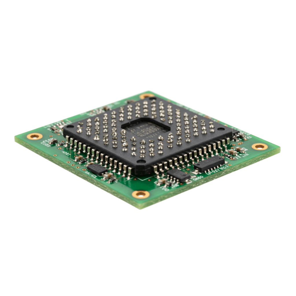
BGA, µBGA, and Ball Grid Arrays
We assemble BGA PCB devices with ball pitch from 1.0 mm down to 0.3 mm using solder mask-defined pads and X-ray validated alignment.
Voiding, head-in-pillow defects, and insufficient solder are minimized through reflow control and paste volume calibration.

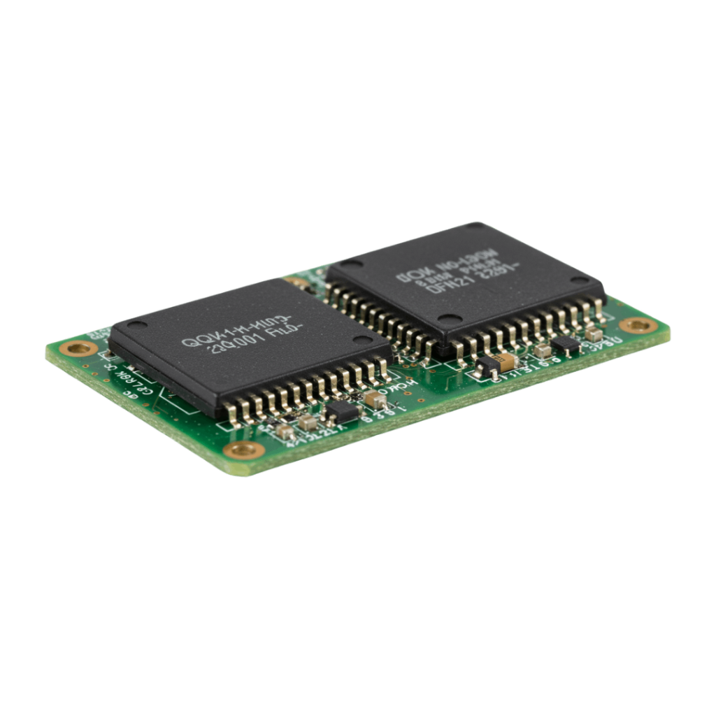
QFN, DFN, and No-Lead Packages
Quad Flat No-Lead and Dual Flat No-Lead packages are handled using x-ray inspection for center pad coverage and perimeter wetting.
We support exposed pad routing with via-in-pad fill and cap processes, especially in fine-pitch circuit layouts with high thermal dissipation needs.

Chip Scale and Ultra-Small ICs
Chip scale packages (CSP) down to 0.4 mm pitch are assembled with controlled paste volume and tight stencil aperture ratios.
These devices require fine-pitch escape routing and impedance-matched pads, especially in high-density PCB assembly applications.

0201, 0402, and Precision Passives
We place passives as small as 0201 on both sides of the printed circuit board, using machine vision to correct skew during rapid placement.
Solder fillet height and pad alignment are verified post-reflow to reduce open joints and false shorts.

Package-on-Package (PoP)
We support PoP stacks by aligning memory and processor dies using optical inspection at each layer. These assemblies require verified planarity, consistent solder volume, and low warpage substrate to maintain coplanar interconnects between stacked components.
How do We Manage Soldering for Fine-Pitch Assemblies?
Soldering in fine pitch PCB assembly requires strict control over paste deposition, thermal gradients, and pad wetting to prevent defects such as bridging, head-in-pillow, or voids. At OurPCB, each fine-pitch assembly run is tailored based on component body size, pitch, copper distribution, and stackup thermal mass to maintain reliable joint formation across high-density interconnects.

Solder Paste Type and Print Uniformity
We use Type 4 paste for pitch ≥0.5 mm and Type 5 solder paste for fine-pitch ICs, PoP, or components below 0.4 mm.
Particle sizes range from 15 to 25 µm for Type 5 to ensure smooth aperture transfer for pads down to 150 µm in width.
Paste volume is verified post-print with 3D solder paste inspection (SPI) to detect low volume (<50% target) or excessive paste that may lead to bridging.
Metal load is maintained between 88 to 89% by weight for print stability on 0.3 mm pitch arrays.

Stencil Design and Aperture Geometry
Stencils are laser-cut stainless steel (tensile strength ≥950 MPa) with electro-polished aperture walls to support uniform paste release. Thickness is application-specific:
- 130 µm for BGA ≥0.5 mm
- 100 µm for fine-pitch components ≤0.4 mm
- 80 µm with step-down zones for 0201 mixed-density designs
Apertures for QFN thermal pads are segmented (e.g. 4x 0.6 mm × 0.6 mm blocks) to control solder volume and avoid voids >25%.
Rounded square and home-plate reductions (5 to 10%) are applied to outer pads of fine-pitch parts to draw fillets without bridging.

Reflow Soldering Profiles
We use 10-zone nitrogen SMT assembly ovens with programmable convection control and zone feedback sensors.
Ramp rate is held below 3 °C/s to reduce CTE mismatch stress, and soak temperatures are set between 150 and 180 °C for flux activation.
Time-above-liquidus (TAL) is kept between 60–90 seconds, with peak reflow at 235–245 °C for SAC305.
For PoP and BGA PCB designs, we limit maximum ΔT between zones to < to prevent warpage and tilt across array pads.

Atmospheric Control and Warpage Prevention
For fine-pitch PCB assembly involving 0201s, CSP, or underfilled BGA, we apply nitrogen reflow (O₂ < 1000 ppm) to reduce oxidation and improve surface wetting.
Boards with asymmetrical copper pour, or partial planes are baked prior to reflow (120 °C, 4 to 6 hrs) to prevent moisture-induced delamination.
Flatness is checked post-reflow on 0.2 mm pitch parts using optical profilometry with warpage limits held to <75 µm across 25 mm span.
How do We Inspect and Test Fine-Pitch PCB Assemblies?
In fine pitch PCB assembly, inspection systems must detect micron-scale defects in solder joints, lead alignment, and pad coverage. At OurPCB, every board passes through sequential inline inspection using SPI, AOI, X-ray, and electrical testing, each calibrated to sub-0.4 mm pitch and high-density interconnect (HDI) layouts. We measure both presence and polarity and solder fillet geometry, X-Y-Z alignment, and subsurface joint quality on every board assembly.

3D AOI for Sub-25 µm Features
Our 3D automated optical inspection (AOI) systems operate with Z-axis resolution to ±5 µm and lateral resolution to 15 µm.
These systems scan every solder joint and pad feature with shape-based algorithms to detect wetting angle deviation, offset leads (>30 µm shift), lifted terminals (>20 µm gap), and incorrect pad-to-pin overlap.
For fine-pitch parts under 0.4 mm, we scan with low-angle light to validate lead coplanarity and fillet volume symmetry.
AOI defect criteria align with IPC-A-610 Class 2 or Class 3, depending on customer requirements.

Solder Paste Inspection (SPI) Before Placement
SPI is applied after stencil printing and before placement using structured light measurement with 2D+3D profile acquisition.
Paste height is measured to ±1 µm accuracy and target volume for fine-pitch pads is held to within ±15% of expected.
For 0.3 mm pitch BGA pads or 0201 component footprints, we enforce minimum paste area coverage of 80% and flag anything under 50% for manual review or stencil cleaning.

X-Ray Inspection for Hidden Solder Terminations
All BGA, µBGA, PoP, and QFN devices undergo 5-axis digital X-ray inspection (AXI) with 2.5 µm per pixel resolution and 360° rotational views for inner pad wetting validation.
We measure ball collapse height, solder joint diameter, and void area (IPC 7095-compliant).
Acceptable void ratio is <25% for power pads and <30% for signal joints.
For ball pitch under 0.4 mm, we inspect for bridging across inner rows and measure diagonal shift between actual and expected pad center within ±75 µm.

In-Circuit and Functional Electrical Testing
ICT coverage includes continuity (0 Ω to 10 MΩ), isolation (>10 MΩ), diode polarity, and voltage threshold detection.
Kelvin testing is used for low-resistance nets (±5 mΩ) in power circuits. For fine-pitch ICs with no exposed leads, a flying probe is used with 300 mm/s travel and ±10 µm probe accuracy to reach via test points and microvias.
Functional test stations simulate power-up, communication protocols, and logic sequence validation on all connectorized outputs.

Traceability and QA Control for Fine-Pitch Assemblies
All inspection data is logged under unit-specific barcodes, linking reflow oven profile ID, stencil lot number, SMT assembly parameters, paste batch code, and operator ID. Defect rates are tracked per stencil aperture set, with SPC charts highlighting recurring issues below 500 ppm.
Boards flagged during SPI, AOI, or X-ray are rerouted through manual inspection under digital microscopes (10x to 50x) or reworked under BGA hot-air stations with thermocouple mapping.


Mon-Fri: 24 hours,
Sat: 9am-6pm, GMT+8

Reach us at
[email protected]
24 hours online

+86-199-30589219
Mon-Fri: 24 hours,
Sat: 9am-6pm, GMT+8
Fine Pitch PCB Assembly FAQs
What is Fine Pitch PCB Assembly?
Fine pitch PCB assembly involves placing and soldering components with a center-to-center lead or ball spacing of 0.5 mm or less, including devices such as BGA, µBGA, QFN, and CSP.
Assemblies in this category use Type 4 or Type 5 solder paste, stencil apertures below 200 µm, and pick-and-place systems with ±25 µm accuracy. The fine-pitch designation also applies to passive footprints like 0201 and 0402, where solder volume and pad wetting must be tightly controlled.
Fine pitch designs require AOI resolution under 15 µm and X-ray inspection for packages with hidden joints, ensuring electrical continuity and thermal stability under high I/O density conditions.
Why does Pitch Matter in PCB Assembly?
Pitch defines the physical space available between adjacent pads or solder balls. In assemblies with 0.4 mm or tighter spacing, this directly impacts trace routing, solder mask clearance, thermal profile symmetry, and inspection access.
For example, a 0.4 mm pitch BGA with full I/O population requires breakout via diameters under 0.25 mm and escape routing with ≤90 µm trace width. Reduced pitch also increases the probability of solder bridging and open leads if stencil aperture design and paste volume are not optimized to ±15% target.
Maintaining proper pad-to-pad separation and avoiding mask slivers is essential to meet IPC-7351 and IPC-A-610 workmanship rules under dense configurations.
What are the Challenges of Fine-Pitch PCB Assembly?
The main challenges in fine-pitch PCB assembly include solder paste control, accurate thermal profiling, and inspection of inaccessible interconnects. In 0.3 mm pitch BGA or QFN packages, aperture clogging and insufficient solder volume often lead to head-in-pillow defects or voids that degrade signal reliability.
Pad coplanarity tolerances under 50 µm must be maintained, and reflow profiles must be set with peak ramp rates under 3 °C/sec to prevent component skew.
Boards with asymmetric copper or multiple plane layers often require pre-baking and nitrogen reflow to prevent delamination or localized overheating, especially in HDI stackups with microvias-in-pad.
What Design Considerations should be followed?
Effective PCB design for fine-pitch assemblies requires strict adherence to pad geometry, escape routing, and material stack selection. For pitch values below 0.5 mm, designers should implement solder mask-defined pads with a 1:1 stencil aperture ratio and maintain trace-to-trace clearance ≥60 µm to meet fabrication minimums.
Thermal pads on QFN packages must be segmented and connected to vias with capped fill to support even reflow. Signal routing beneath fine-pitch components should preserve controlled impedance through continuous reference planes and matched trace widths (e.g. 85 to 90 µm for 50 Ω single-ended).
The entire design must be reviewed against the assembler’s fabrication tolerances, including annular ring size and copper thickness at breakout layers.
Do You Support Turnkey and Volume Production?
Yes, OurPCB offers full turnkey support for fine-pitch assembly, including component sourcing, stencil fabrication, board production, and final test. We handle low-to-mid volume builds involving sub-0.4 mm pitch BGA, PoP stack integration, and dual-sided SMT on rigid, flex, and hybrid substrates.
All components are procured from traceable suppliers and logged under moisture sensitivity level (MSL) protocols, with drying and vacuum sealing applied where required.
Our production lines support serialized traceability, Class III visual inspection, and lot-based X-ray verification for hidden pad joints. This end-to-end process is supported by operator-level SPC tracking and automated yield reporting at each QA checkpoint.
Ready to Build Fine-Pitch PCB Assemblies With Confidence?
OurPCB delivers high-precision fine pitch PCB assembly services with support for sub-0.4 mm pitch devices, BGA and PoP integration, and inline inspection across every stage of the assembly process. Send us your Gerber files, BOM, and technical requirements to receive a detailed quote from our engineering team.