Top 10 Classic Car Wiring Harness Manufacturers | Full Guide
Finding the right wiring harness manufacturer for your vintage ride can be a real headache. Those beautiful old machines need special wiring that looks period-correct

EV charger PCBs operate under high current, elevated temperatures, and strict regulatory constraints. They form the electrical and control backbone of AC, DC, and fast-charging systems, managing power conversion, communication, thermal dissipation, and fault protection.
OurPCB manufactures AC, DC, and hybrid EV charger designs with printed circuit boards built to withstand continuous field exposure, fluctuating load cycles, and compliance requirements, including IEC 61851 and ISO 15118.


Choosing the right PCB manufacturer for EV chargers means more than just hitting specifications; it’s about consistent quality, fast lead times, and a partner who understands the regulatory and reliability pressures of electric vehicle infrastructure. OurPCB delivers that foundation across every layer of design and production.


OurPCB operates two fully equipped manufacturing sites in China, each covering over 10,000 square meters of production space.
These facilities are built to support high-volume EV charger PCB assembly across SMT, THT, and hybrid processes. Both sites are vertically integrated, allowing for seamless control over fabrication, assembly, testing, and final packaging.
Production lines are outfitted with advanced equipment, including solder paste printers, reflow ovens, AOI systems, BGA rework stations, and ICT testers. Dedicated zones are maintained for nitrogen reflow, X-ray inspection, and conformal coating to support high-voltage PCB applications in EV charging systems.

OurPCB manufactures EV charger PCBs in facilities certified to ISO 9001:2015 and IATF 16949:2016, meeting the requirements for automotive and high-reliability electronics.
We build to IPC-A-610 Class 2 by default, with full capability for Class 3 when higher durability or safety margins are required.
Our engineering workflows also support PCB assembly projects targeting IEC 61851 and ISO 15118, a smart charging protocol enabling EV authentication via the control pilot line.

Since 2007, OurPCB has delivered precision PCB assembly services to over 3,000 customers across 40 countries.
Our client base spans electric vehicle manufacturers, automotive Tier 1 suppliers, charging infrastructure developers, and industrial energy OEMs. This depth of experience enables us to meet the performance, cost, and compliance expectations of global EV programs.
We support both prototype and mass production needs, with structured NPI workflows and repeatable process controls.
Clients rely on our technical stability, fast response times, and consistent output across multilayer charger boards, control PCBs, and power regulation modules.

OurPCB provides full engineering support to streamline EV charger PCB design and accelerate production readiness.
Our in-house team reviews all Gerber files, BOMs, and stack-ups for manufacturability, focusing on high-voltage isolation, trace current capacity, and controlled impedance requirements.
We assist with impedance matching, conductor width calculations, and interlayer clearance analysis to meet the demands of AC and DC charger designs.
For complex builds, we offer design feedback for structures, thermal reliefs, and pad geometries, along with guidance on compliance with IPC, IEC, and regional safety standards.

OurPCB sources all components for EV charger PCB assemblies from authorized global distributors, including Mouser, Digi-Key, Future Electronics, and WPG.
We manage lifecycle status, lead time risk, and cross-referencing to ensure stable sourcing for automotive-grade components such as SiC MOSFETs, gate drivers, current sensors, and power supply ICs.
All incoming materials are subject to ESD-safe handling, lot-level inspection, and barcode tracking throughout the assembly process.

OurPCB supports rapid program timelines with fast and accurate quoting for EV charger PCB builds.
Standard quotes for bare PCB fabrication are delivered within 8 working hours, while full turnkey PCBA quotes with component sourcing are provided within 48 hours.
Our staff works directly with engineers and procurement teams to resolve DFM questions, confirm delivery schedules, and manage revisions across global time zones.


OurPCB operates two fully equipped manufacturing sites in China, each covering over 10,000 square meters of production space.
These facilities are built to support high-volume EV charger PCB assembly across SMT, THT, and hybrid processes. Both sites are vertically integrated, allowing for seamless control over fabrication, assembly, testing, and final packaging.
Production lines are outfitted with advanced equipment, including solder paste printers, reflow ovens, AOI systems, BGA rework stations, and ICT testers. Dedicated zones are maintained for nitrogen reflow, X-ray inspection, and conformal coating to support high-voltage PCB applications in EV charging systems.
Since 2007, OurPCB has delivered precision PCB assembly services to over 3,000 customers across 40 countries.
Our client base spans electric vehicle manufacturers, automotive Tier 1 suppliers, charging infrastructure developers, and industrial energy OEMs. This depth of experience enables us to meet the performance, cost, and compliance expectations of global EV programs.
We support both prototype and mass production needs, with structured NPI workflows and repeatable process controls.
Clients rely on our technical stability, fast response times, and consistent output across multilayer charger boards, control PCBs, and power regulation modules.
OurPCB provides full engineering support to streamline EV charger PCB design and accelerate production readiness.
Our in-house team reviews all Gerber files, BOMs, and stack-ups for manufacturability, focusing on high-voltage isolation, trace current capacity, and controlled impedance requirements.
We assist with impedance matching, conductor width calculations, and interlayer clearance analysis to meet the demands of AC and DC charger designs.
For complex builds, we offer design feedback for structures, thermal reliefs, and pad geometries, along with guidance on compliance with IPC, IEC, and regional safety standards.
OurPCB sources all components for EV charger PCB assemblies from authorized global distributors, including Mouser, Digi-Key, Future Electronics, and WPG.
We manage lifecycle status, lead time risk, and cross-referencing to ensure stable sourcing for automotive-grade components such as SiC MOSFETs, gate drivers, current sensors, and power supply ICs.
All incoming materials are subject to ESD-safe handling, lot-level inspection, and barcode tracking throughout the assembly process.
OurPCB supports rapid program timelines with fast and accurate quoting for EV charger PCB builds.
Standard quotes for bare PCB fabrication are delivered within 8 working hours, while full turnkey PCBA quotes with component sourcing are provided within 48 hours.
Our staff works directly with engineers and procurement teams to resolve DFM questions, confirm delivery schedules, and manage revisions across global time zones.
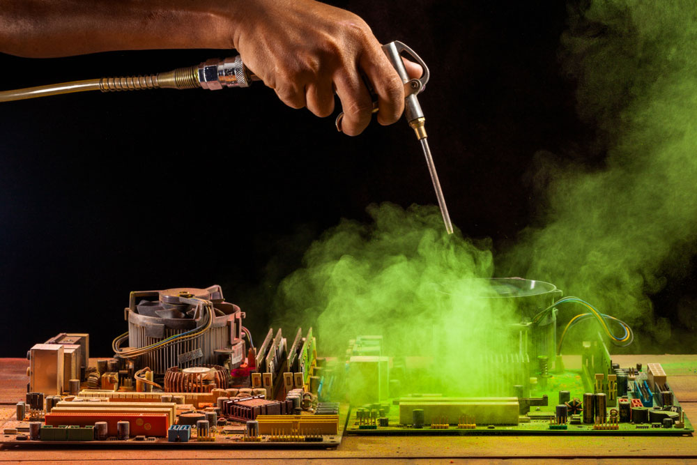
At OurPCB, we remove no-clean flux during the PCBA cleaning process to prevent insulation resistance loss, support coating adhesion, and avoid inspection rejection in Class 2 and 3 assemblies.
Although low-solid no-clean flux is engineered to remain on the board, its residue absorbs moisture, lowers surface resistivity, and disrupts conformal coating uniformity, especially near component edges or mask-defined pads.
Our PCBA cleaning procedures are based on flux type, component density, and coating thickness requirements, and are qualified using ionic cleanliness testing, white residue detection, and surface preparation metrics that ensure coating and inspection compliance.
We remove no-clean flux residue because its remaining solids form hygroscopic films with ionic content capable of enabling leakage currents under bias. These residues often contain halide activators or rosin derivatives that, in humid environments, allow ionic mobility as low as 10⁸ Ω insulation resistance across narrow conductor spacing.
On high-density printed circuit board assemblies, especially those with ≤0.3 mm pitch, this can lead to dendritic growth, moisture-induced tracking, and eventual open or short failures. In Class 3 applications, even visually benign residues violate IPC J-STD-001 Section 8.3.1, prohibiting any visible residue under conformal coating.
Removing these residues is required to maintain dielectric performance and prevent latent field degradation.
Our cleaning strategy depends on the flux chemistry and board design. For fully assembled SMT boards, we use vapor degreasing with HFE-72DA or Vertrel XF, which condense at 55 °C – 65 °C onto the PCBA surface, dissolve polar and non-polar residues, and evaporate without leaving water or exposing components to immersion.
In rework areas or where selective cleaning is required, we use Decotron T383 or high-purity IPA with aerosol precision nozzles to rinse solder ball traps and low-solids residue from around pads.
The process is followed by 30 psi filtered air drying or vacuum-assisted drying to prevent water adsorption beneath packages. Surface prep is validated using surface insulation resistance (SIR) measurements, ionic testing (<1.56 µg/cm² NaCl equivalent), and UV light to detect fluorescence from missed residues.
Removing flux residue allows for consistent conformal coating flow and edge adhesion, especially in boards using urethane or acrylic coatings. Cleaned surfaces increase surface energy, improving film wetting and eliminating common defects like dewetting, bridging, or edge lift.
Coating adhesion strength improves from 1.2 N/mm (on flux-contaminated surfaces) to over 2.5 N/mm on properly cleaned copper and solder mask regions, reducing delamination risk during thermal cycling. In addition, a clean PCB surface ensures that automated optical inspection (AOI), UV inspection, or manual visual checks can accurately detect voids, bubbles, or skipped areas.
For applications in automotive ECUs, implantable medical devices, or high-speed digital RF systems, surface cleanliness before coating directly correlates to long-term device reliability in harsh conditions.
EV charger designs require boards that balance electrical performance with thermal, mechanical, and compliance demands. Here’s how OurPCB meets those challenges through advanced fabrication, materials selection, and topology-specific design support.
OurPCB fabricates EV charger (electric vehicle charger) PCBs from 2 to 32 layers, including rigid, flex, and rigid-flex stack-ups. Standard builds use FR4 or high-Tg FR4 (up to 180 °C Tg), with support for halogen-free, ceramic-filled, and polyimide substrates where thermal resistance or insulation integrity is required. Hybrid builds combining FR4 and PTFE or ceramic layers can be produced up to 16 layers with engineering review.
We support overall board thicknesses from 0.2 mm to 8.0 mm, with finished copper weights from 1/3 oz to 15 oz. Internal copper distribution is engineered to manage layer-specific current loads in AC or DC power sections, with stack-up validation provided for impedance matching and creepage (surface spacing between conductors to prevent arcing) compliance.e. Dielectric materials include ITEQ IT180A, Isola 370HR, and TUC TU-872 for high-voltage durability and low Dk stability across frequency.
OurPCB supports tight dimensional control and fine-feature fabrication for EV charger PCBs operating at high voltage and high current. Standard trace widths and spacing down to 0.05 mm (2 mil) are achievable with LDI exposure and precision etching, depending on copper weight and layer count. For inner layers, 3/3 mil design rules are supported on 35 µm copper; outer layers can reach 2.5/2.5 mil with 30 µm finished copper.
Minimum mechanical drill diameter is 0.15 mm, with aspect ratios up to 10:1 for plated through holes. Via-in-pad, back drilling, and controlled-depth milling are available for fine pitch designs and high-speed signal routing. Board outline tolerances are held to ±0.1 mm, with hole position accuracy to ±0.075 mm.
Standard thickness tolerance is ±10% for boards ≤1.0 mm and ±7% for boards between 1.8 mm and 4.0 mm. All fabrication steps are governed by IPC-6012 and IPC-2221 design standards for Class 2 and Class 3 performance targets.
Standard finishes include lead-free HASL, OSP, ENIG, immersion silver, immersion tin, and hard gold plating. These options are selected based on end-use application, required contact durability, and environmental exposure.
ENIG (Electroless Nickel Immersion Gold), a corrosion-resistant nickel-gold surface finish, provides excellent planarity and corrosion resistance, making it ideal for connector pads and surface-mounted components in AC and DC charging modules. Immersion silver is available for high-speed signal layers requiring low contact resistance. Hard gold is used for edge connectors or gold fingers subjected to repeated mechanical wear.
All surface finishes are RoHS-compliant and applied in controlled chemical environments with line-level inspection for thickness, solderability, and uniformity. Selective finish combinations, such as ENIG with hard gold edge fingers or OSP over inner copper layers, are supported to meet mixed interface requirements in EV charging systems.
OurPCB provides end-to-end assembly services for EV charger PCBs, supporting both surface mount and through-hole technologies. SMT lines handle fine-pitch components down to 0201 packages, with placement accuracy of ±25 µm and reflow profiles optimized for multilayer high-copper boards. Nitrogen reflow is available for oxidation-sensitive assemblies, especially in high-voltage applications.
We support THT processes for connectors, relays, and large passive components using wave soldering or selective soldering with controlled thermal gradients. Double-sided reflow, mixed technology, and BGA rework services are also available. BGAs are aligned using optical centering and inspected post-process with 5 µm resolution X-ray systems.
All assembly steps follow IPC-A-610 Class 2 or Class 3 criteria, with real-time process monitoring for solder paste volume, placement alignment, and joint integrity. ESD-safe material handling, moisture-sensitive device (MSD) tracking, and batch-level lot control are standard across both facilities.
OurPCB integrates inline inspection and electrical test systems throughout the EV charger PCB assembly process to verify build quality, functional integrity, and regulatory compliance. Automated Optical Inspection (AOI) is used after solder paste printing and post-reflow to detect component skew, tombstoning, insufficient solder, and polarity errors across all SMT placements.
For assemblies with BGAs, QFNs, or embedded pads, real-time X-ray inspection validates solder joint formation and detects voids, bridging, or incomplete wetting. All BGA rework is re-inspected post-process. Solder paste inspection (SPI) verifies volume, height, and area coverage before pick-and-place.
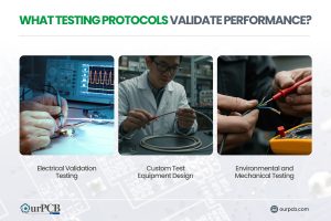
In-circuit testing (ICT) is available for populated PCBs with accessible test points, using custom fixtures to measure continuity, resistance, diode orientation, and component presence. High-voltage testing and functional test rigs can be applied at end-of-line for charger boards operating in 220V or 380V systems. All tests follow IPC-TM-650 and customer-specific protocols for yield control and traceability.
OurPCB offers protective coating and environmental sealing solutions tailored to the outdoor and high-voltage demands of EV charger PCBs. Conformal coating, a protective film that shields against humidity, dust, and ionic contamination, is applied by selective spray, dip, or brushing methods using acrylic, silicone, or polyurethane chemistries. These coatings protect against humidity, condensation, dust, and ionic contamination, with thickness control between 25 µm and 75 µm.
We also provide three-proof treatment—moisture-proof, mold-proof, and salt-spray-proof—based on GB/T 4797.6-1995 standards. This process enhances board survivability in outdoor-rated chargers subject to IP54 or IP65 enclosures. Materials are qualified for adhesion, dielectric strength, and thermal cycling resistance.
All coated boards are UV-inspected for coverage uniformity and undergo post-cure verification before final packaging. Optional masking is available for connectors, test points, or edge fingers to maintain electrical interface integrity during the coating process.
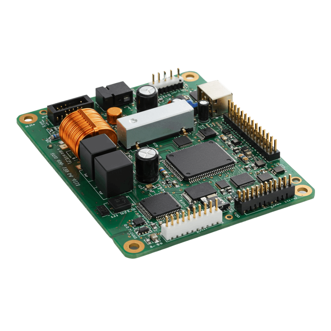
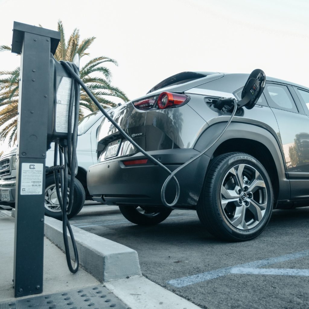
OurPCB manufactures EV charger PCBs designed for AC, DC, and AC/DC integrated systems, supporting charger power levels from 3.3 kW up to 30 kW. We fabricate control and power conversion boards for AC Level 1 and Level 2 chargers, DC fast chargers, and bidirectional onboard modules. Each topology requires specific copper distribution, insulation spacing, and thermal design strategies incorporated at the stack-up and layout levels.
For AC designs, we support isolated control PCBs with precise routing for zero-crossing detection, relay actuation, and grid interface circuitry. DC charger PCBs are built for direct high-current transfer, with wide trace widths, heavy copper layers, and reinforced dielectric spacing to meet safety class clearance requirements.
We also support charger architectures using SiC MOSFETs, GaN FETs, and phase-shifted full bridge (PSFB), LLC, or dual active bridge (DAB) converter topologies. Our production team can adapt layer counts, thermal relief, and pad geometry to support each topology’s electrical and mechanical demands.
EV charger designs require boards that balance electrical performance with thermal, mechanical, and compliance demands. Here’s how OurPCB meets those challenges through advanced fabrication, materials selection, and topology-specific design support.
OurPCB fabricates EV charger (electric vehicle charger) PCBs from 2 to 32 layers, including rigid, flex, and rigid-flex stack-ups. Standard builds use FR4 or high-Tg FR4 (up to 180 °C Tg), with support for halogen-free, ceramic-filled, and polyimide substrates where thermal resistance or insulation integrity is required. Hybrid builds combining FR4 and PTFE or ceramic layers can be produced up to 16 layers with engineering review.
We support overall board thicknesses from 0.2 mm to 8.0 mm, with finished copper weights from 1/3 oz to 15 oz. Internal copper distribution is engineered to manage layer-specific current loads in AC or DC power sections, with stack-up validation provided for impedance matching and creepage (surface spacing between conductors to prevent arcing) compliance.e. Dielectric materials include ITEQ IT180A, Isola 370HR, and TUC TU-872 for high-voltage durability and low Dk stability across frequency.
OurPCB supports tight dimensional control and fine-feature fabrication for EV charger PCBs operating at high voltage and high current. Standard trace widths and spacing down to 0.05 mm (2 mil) are achievable with LDI exposure and precision etching, depending on copper weight and layer count. For inner layers, 3/3 mil design rules are supported on 35 µm copper; outer layers can reach 2.5/2.5 mil with 30 µm finished copper.
Minimum mechanical drill diameter is 0.15 mm, with aspect ratios up to 10:1 for plated through holes. Via-in-pad, back drilling, and controlled-depth milling are available for fine pitch designs and high-speed signal routing. Board outline tolerances are held to ±0.1 mm, with hole position accuracy to ±0.075 mm.
Standard thickness tolerance is ±10% for boards ≤1.0 mm and ±7% for boards between 1.8 mm and 4.0 mm. All fabrication steps are governed by IPC-6012 and IPC-2221 design standards for Class 2 and Class 3 performance targets.
Standard finishes include lead-free HASL, OSP, ENIG, immersion silver, immersion tin, and hard gold plating. These options are selected based on end-use application, required contact durability, and environmental exposure.
ENIG (Electroless Nickel Immersion Gold), a corrosion-resistant nickel-gold surface finish, provides excellent planarity and corrosion resistance, making it ideal for connector pads and surface-mounted components in AC and DC charging modules. Immersion silver is available for high-speed signal layers requiring low contact resistance. Hard gold is used for edge connectors or gold fingers subjected to repeated mechanical wear.
All surface finishes are RoHS-compliant and applied in controlled chemical environments with line-level inspection for thickness, solderability, and uniformity. Selective finish combinations, such as ENIG with hard gold edge fingers or OSP over inner copper layers, are supported to meet mixed interface requirements in EV charging systems.
OurPCB provides end-to-end assembly services for EV charger PCBs, supporting both surface mount and through-hole technologies. SMT lines handle fine-pitch components down to 0201 packages, with placement accuracy of ±25 µm and reflow profiles optimized for multilayer high-copper boards. Nitrogen reflow is available for oxidation-sensitive assemblies, especially in high-voltage applications.
We support THT processes for connectors, relays, and large passive components using wave soldering or selective soldering with controlled thermal gradients. Double-sided reflow, mixed technology, and BGA rework services are also available. BGAs are aligned using optical centering and inspected post-process with 5 µm resolution X-ray systems.
All assembly steps follow IPC-A-610 Class 2 or Class 3 criteria, with real-time process monitoring for solder paste volume, placement alignment, and joint integrity. ESD-safe material handling, moisture-sensitive device (MSD) tracking, and batch-level lot control are standard across both facilities.
OurPCB integrates inline inspection and electrical test systems throughout the EV charger PCB assembly process to verify build quality, functional integrity, and regulatory compliance. Automated Optical Inspection (AOI) is used after solder paste printing and post-reflow to detect component skew, tombstoning, insufficient solder, and polarity errors across all SMT placements.
For assemblies with BGAs, QFNs, or embedded pads, real-time X-ray inspection validates solder joint formation and detects voids, bridging, or incomplete wetting. All BGA rework is re-inspected post-process. Solder paste inspection (SPI) verifies volume, height, and area coverage before pick-and-place.
In-circuit testing (ICT) is available for populated PCBs with accessible test points, using custom fixtures to measure continuity, resistance, diode orientation, and component presence. High-voltage testing and functional test rigs can be applied at end-of-line for charger boards operating in 220V or 380V systems. All tests follow IPC-TM-650 and customer-specific protocols for yield control and traceability.
OurPCB offers protective coating and environmental sealing solutions tailored to the outdoor and high-voltage demands of EV charger PCBs. Conformal coating, a protective film that shields against humidity, dust, and ionic contamination, is applied by selective spray, dip, or brushing methods using acrylic, silicone, or polyurethane chemistries. These coatings protect against humidity, condensation, dust, and ionic contamination, with thickness control between 25 µm and 75 µm.
We also provide three-proof treatment—moisture-proof, mold-proof, and salt-spray-proof—based on GB/T 4797.6-1995 standards. This process enhances board survivability in outdoor-rated chargers subject to IP54 or IP65 enclosures. Materials are qualified for adhesion, dielectric strength, and thermal cycling resistance.
All coated boards are UV-inspected for coverage uniformity and undergo post-cure verification before final packaging. Optional masking is available for connectors, test points, or edge fingers to maintain electrical interface integrity during the coating process.
OurPCB manufactures EV charger PCBs designed for AC, DC, and AC/DC integrated systems, supporting charger power levels from 3.3 kW up to 30 kW. We fabricate control and power conversion boards for AC Level 1 and Level 2 chargers, DC fast chargers, and bidirectional onboard modules. Each topology requires specific copper distribution, insulation spacing, and thermal design strategies incorporated at the stack-up and layout levels.
For AC designs, we support isolated control PCBs with precise routing for zero-crossing detection, relay actuation, and grid interface circuitry. DC charger PCBs are built for direct high-current transfer, with wide trace widths, heavy copper layers, and reinforced dielectric spacing to meet safety class clearance requirements.
We also support charger architectures using SiC MOSFETs, GaN FETs, and phase-shifted full bridge (PSFB), LLC, or dual active bridge (DAB) converter topologies. Our production team can adapt layer counts, thermal relief, and pad geometry to support each topology’s electrical and mechanical demands.
EV charger PCBs require substrate materials with high thermal stability, strong dielectric properties, and consistent electrical performance under load. For most AC and DC charger designs, high-Tg FR4 laminates rated to ≥170 °C prevent delamination and dielectric breakdown during continuous operation. Standard options include ITEQ IT180A, TUC TU-883, and Isola 370HR, all qualified for high voltage and thermal cycling.
For high-frequency or bidirectional power conversion modules, we select low-loss materials such as Rogers RO4003C or Panasonic R-5785 to minimize signal attenuation and dielectric heating. These materials offer low Dk drift and reduced loss tangent, supporting gate driver signals, feedback loops, and CAN/LIN interfaces in EV charger control boards.
Copper thickness is 1 oz to 3 oz for inner layers and up to 15 oz for external power planes in high-current DC output paths. To support these copper weights, we apply a thicker solder mask (eg. 15 to 25 µm dry film or 25 to 50 µm liquid photoimageable mask) to maintain electrical isolation. Solder masks conform to IPC-SM-840 Class T or H specifications, depending on coating type and required voltage.
Understanding different EV charger types helps explain the electrical, thermal, and structural demands placed on their supporting PCBs.
| Charging Type | Power Range | Conversion Location | Typical Use Case | PCB Design Implications |
|---|---|---|---|---|
| AC Level 1 | 1.4 kW (120V, 12A) | Inside the vehicle (onboard charger) | Home or personal use | Low-current traces, basic insulation, minimal thermal load |
| AC Level 2 | 3.3 to 22 kW (240V) | Inside the vehicle | Residential and commercial wall-mounted units | Multi-layer boards with isolation zones, EMI filtering, thermal relief for relays and SSRs |
| DC Fast Charging | 50 to 350 kW | Inside the charger (offboard) | Highway stations, fleet depots | Heavy copper (≥3 oz), wide power planes, thick solder mask, creepage/clearance spacing |
| AC/DC Integrated | 7 to 30 kW | Split (control + rectification) | Wall or pedestal chargers (multimode) | Mixed-signal layout, high voltage isolation, stack-up balancing, combined power/control PCBs |
EV charger PCBs are used in both fixed and onboard charging systems, with design requirements that vary by deployment environment, installation method, and end-user access.
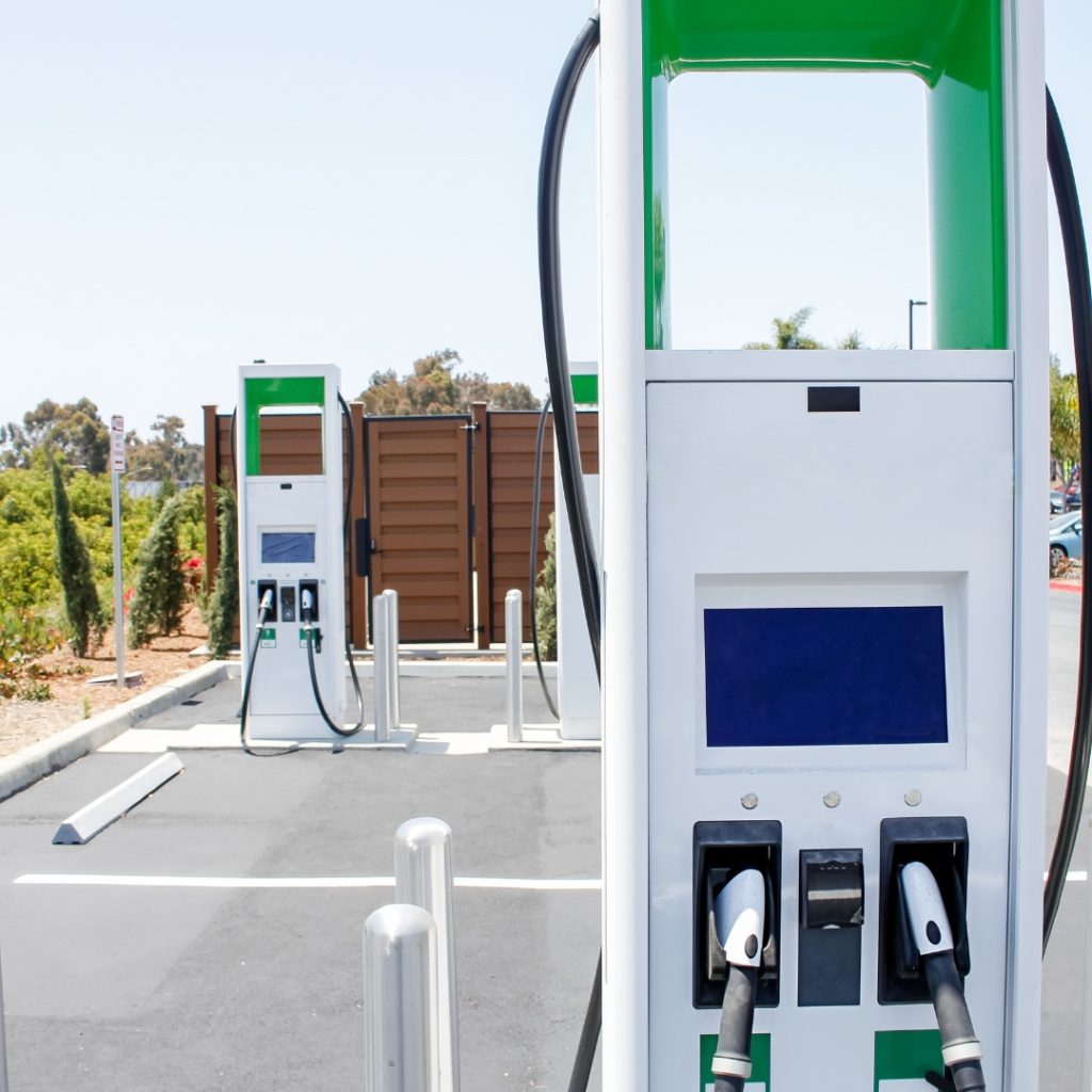
These units operate outdoors and require PCBs built with conformal coating, high-voltage spacing, and weatherproofed connectors. Power control boards manage AC grid input and drive DC output modules at levels from 50 kW to 350 kW.
Wall-mounted or portable, these systems use lower-power PCBs (3.3 to 7 kW) that focus on safety, compact layout, and efficient thermal design. EMI suppression and reinforced insulation spacing are necessary for safe operation in confined or enclosed environments.
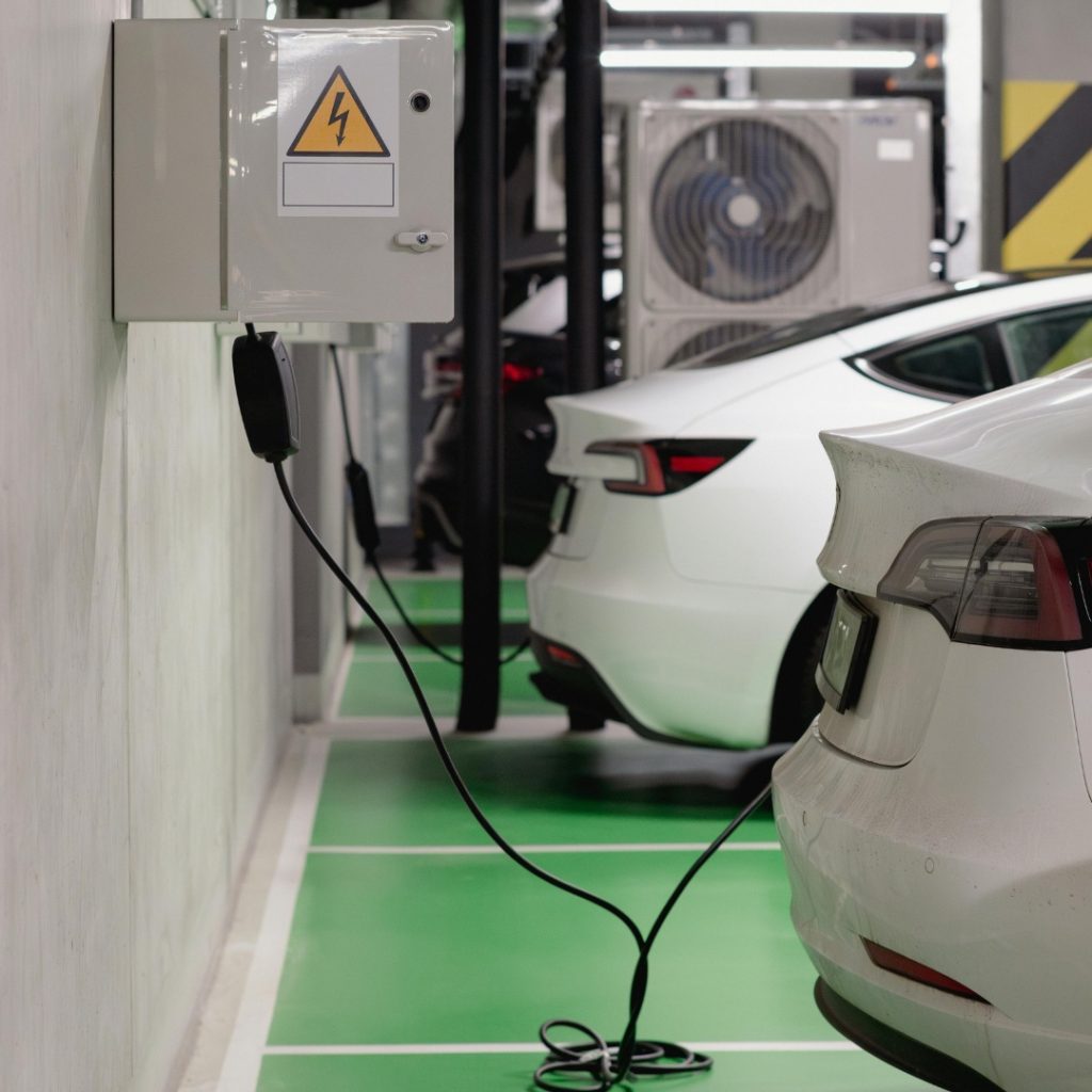
Chargers installed in logistics yards or bus terminals require scalable PCBs designed for load balancing, vehicle authentication, and power management across multiple outputs. These boards integrate monitoring circuits and support higher duty cycles
Installed within the vehicle, these PCBs convert AC to DC internally and require compact, thermally stable designs. They must interface directly with vehicle battery systems and comply with ISO 15118 and CAN bus communication requirements.
Mon-Fri: 24 hours,
Sat: 9am-6pm, GMT+8
Reach us at
[email protected]
24 hours online
+86-199-30589219
Mon-Fri: 24 hours,
Sat: 9am-6pm, GMT+8
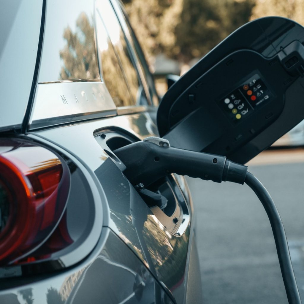
An EV charger PCB is the primary circuit board that controls power conversion, safety interlocks, and communication between the charging station and electric vehicle. It routes high voltage and current across isolated paths, manages control logic, and interfaces with the charger’s relay, sensor, and pilot circuits.
Without a properly designed PCB, the charger cannot regulate output, meet insulation standards, or support compliant communication with the vehicle.
EV charger PCB assembly includes surface mount and through-hole component placement, soldering, inspection, and testing. SMT parts are placed using pick-and-place machines and reflow soldered in nitrogen ovens.
Power devices and connectors are wave or selectively soldered. BGAs and QFNs are X-ray inspected, and high-voltage boards are HiPot tested post-assembly. The process includes solder paste inspection (SPI), AOI, and moisture-sensitive component handling.
EV charger PCBs must comply with both electrical safety and communication standards to ensure reliable operation and regulatory acceptance. The two primary global frameworks are IEC 61851 and ISO 15118.
IEC 61851 defines charging modes, insulation spacing, fault detection, and protection levels for EV supply equipment. It specifies the minimum creepage and clearance distances based on working voltage, pollution degree, and overvoltage category. Charger PCB layouts must account for these values in both coated and uncoated conditions, often requiring ≥3.2 mm creepage for 230V AC circuits without conformal coating.
ISO 15118 supports secure digital communication between the EV and the charger, enabling user authentication, billing integration, and Plug & Charge functionality. Our charger PCBs accommodate these requirements using physical-layer PLC coupling, digital logic isolation, and EMI-filtered signal lines.
Regional standards such as SAE J1772 (North America) and IEC 62196 (Europe) also influence connector pinout, control signal timing, and electrical isolation requirements. These impact board-level design for pilot signal generation, relay control, and error detection circuits.
OurPCB delivers certified, high-reliability EV charger PCB assembly services for AC, DC, and hybrid charging systems.
Contact us today to start your next EV charger PCB project and receive a quote within 8 to 48 hours.
Finding the right wiring harness manufacturer for your vintage ride can be a real headache. Those beautiful old machines need special wiring that looks period-correct
Would your car be able to run without wire harnesses? Not a chance. Wire harnesses connect all the electrical parts together. No harness means no
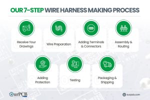
Making wire harnesses isn’t complicated. At OurPCB, we create custom wire harnesses for an expansive range of industries every day. While it’s a complicated process,
Prototype cable assemblies are the very important place in between PCB design ideas and interconnects. OurPCB brings prototype assemblies with PCB solutions to your tables.
PCB thermal management prevents component overheating through strategic heat transfer techniques. Without proper thermal control, electronics are at risk of electronic failures through weakened solder
ContentsKey TakeawaysWhat is a Multilayer-Printed Circuit Board?How do Multilayer PCB Boards Work?Multilayer PCB ApplicationsMultilayer PCB Manufacturing Process: StepsMultilayer PCB Manufacturing MachinesBenefits of Multilayer Circuit BoardsWhat
We use cookies to improve your browsing experience, which may include personal information. By clicking "Agree," you accept our Privacy Policy and cookie use. You can change your cookie settings in your browser anytime.
Agree
 Chat With Us
 Free Quote