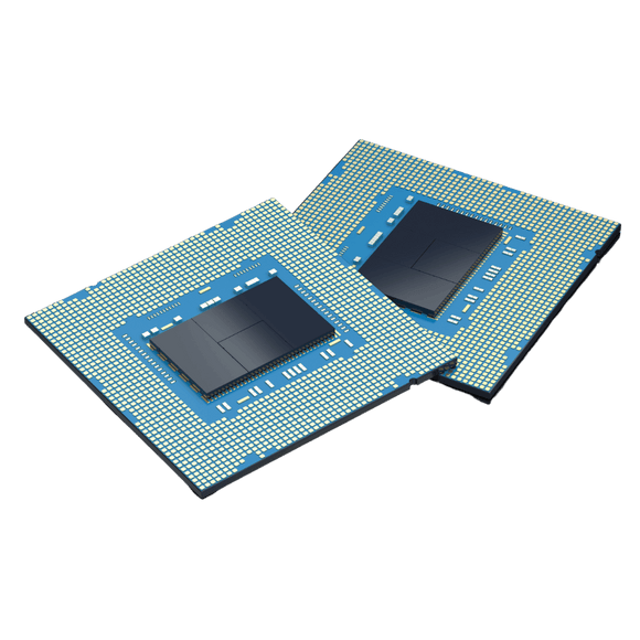
Start by choosing a suitable ball pitch—larger pitches like 1.0 mm are easier to route and inspect than fine-pitch BGAs. Use non-solder mask defined (NSMD) pads to improve solder joint quality and avoid open vias under pads unless they’re filled and capped to prevent solder wicking.
Maintain proper trace width and spacing based on your manufacturer’s design rules, and plan your layer stackup to allow clean escape routing—using microvias for high-density layouts. Keep solder mask alignment tight, apply the right paste volume, and leave space for test points or JTAG access since BGA joints can’t be visually inspected.


