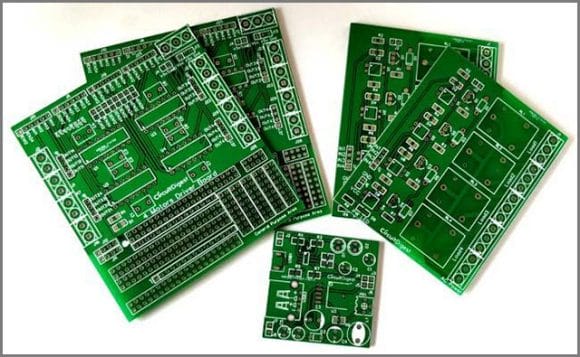
Blog  /  Ultimate Guide to Custom PCBs

Ultimate Guide to Custom PCBs

PCB boards are all around us in every gadget we use. Be it a smartphone or a simple calculator; their function depends on the performance of PCBs. Do you know what the PCB circuit boards are made of? PCB vs. PCBA-What is the differences? Have you ever opened up your iPhone to see what's inside? […]
Special Offer Get $100off your order!
Claim your $100 discount by sending an inquiry today. Act now to save on your next project! Please email [email protected] for details.
Quote Form
check whiteFastcheck whiteExciting Dealscheck whiteFree
1 2 3
Table of Contents

PCB boards are all around us in every gadget we use. Be it a smartphone or a simple calculator; their function depends on the performance of PCBs.

Do you know what the PCB circuit boards are made of?

PCB vs. PCBA-What is the differences?

Have you ever opened up your iPhone to see what's inside?

You would find only a few things, from the digitizer and battery to soldering and, of course, the PCB.

The logic board keeps your iPhone running, and any damage to it results in your phone being unable to power on again.

For instance, the compact circuit board design of the iPhone X has wowed many analysts and techies. It is a feat of engineering that not many companies have been able to surpass.

So, what is it that makes circuit boards so unique?

What makes one circuit board better than the other?

What does a circuit board consist of?

No worries!

We have prepared this helpful guide where you can learn about the materials used to make PCBs.

You can also get a picture of how a manufacturer produces them. Let's begin by looking at what the circuit boards are made of.

Then, we will look at how you can make your circuit boards.

At the end of this article, we will guide you through the path to ensuring that you get the best from the right vendor.

Special Offer: Get $100 off your order!

Claim your $100 discount by sending an inquiry today. Act now to save on your next project!
Please email [email protected] for details.

What are PCBs?

PCBs are also known as printed circuit boards, and they are the driving components of the different electronics and electrical equipments or tools we use daily.

Most PCBs are formed by combining two or more layers depending upon the complexity and nature of the device they are used in.

What Materials are Used in Printed Circuit Boards?

PCBs use a variety of materials for their composition. A layer can be made from fiberglass or resin derived from paper while other materials, such as copper, solder mask, and silkscreen layers, are also used.

Samples of Custom PCBs


PCB BoardsPCB is generally made from four layers bonded by heat, pressure, and other methods. Four PCB layers are made of the substrate, copper, solder mask, and silkscreen.

The PCB materials encompassed by the printed circuit board includes:

Copper

Copper is used on the thick layer of foundation known as the substrate. Depending on the board type and use, one or two copper layers can be present. The copper layer can exist on one side of the PCB, or it may be present on both sides of the substrate.

Simple electronic devices use PCBs, which have a copper layer only on one side. Copper layers are much thinner and more delicate than the substrate.The copper used in PCBs is referred to by weight and presented in ounces per square foot .Most common PCBs come with a copper content of 1 ounce of copper per square foot.

The amount of copper in the PCB determines the amount of power it utilizes.

Silkscreen

Silkscreen is responsible for making the printed circuit board readable to technology programmers by adding numerical and letter indicators.

Substrate

The substrate is known as FR4, an acronym for Fire Retardant.
It provides a thick layer of foundation for the printed circuit board, which varies. However, you will find their thickness changes. It is the layer that offers rigidity to the PCB. It can also be made from flexible materials, which can sometimes be stretched. Recently many innovative materials have been used to create the substrate, some of which are plant-based.

The substrate is generally made of fiberglass, also known as FR4. FR refers to the fire retardant and provides the foundation of the PCB. The substrate layer is the thickest in any PCB

Some other materials are also used for making the substrate, such as epoxy or phenolics.

Soldermask

A green top layer of PCB is known as the solder mask and is applied over the copper layer to contact other electrical parts.

Custom PCB

PCB Materials to Avoid

It is important to note that other board types do not use the above-listed materials. Instead, they make use of epoxies. A disadvantage attached to this type of commission is that they are thermally sensitive, making them susceptible to fast loss of their lamination.

One way to recognize this type of board is through the smell they give when undergoing soldering.

The boards made from epoxy resin suffer thermal sensitivity, and the lamination can sometimes fade quickly.

You can find these cost-effective boards easily in the market and recognize them by the smell they give off.

The material also needs the components to be soldered to it.

Printed circuit board - shielding material

Special Offer: Get $100 off your order!

Claim your $100 discount by sending an inquiry today. Act now to save on your next project!
Please email [email protected] for details.

Types of PCB

As briefed earlier, the PCB is a crucial component in different electronics. Now, let's consider the masterpiece behind your TV set and remote; the TV set can change channels from a press on the remote due to the presence of a kind of PCB in the remote.

There are many applications of the PCB which ease our very existence and make our daily activities flexible.

Depending on the use, PCB manufacturers use varying types of PCB to suit different products. The type of printed circuit board includes;

Single-sided PCB

In the earlier part of this article, we mentioned that the substrate varies with use. In the single-sided type of PCB, the substrate contained is just one.

A suitable electrical conductor such as copper is used to shield a side of the substrate, the solder mask is present on the copper layer, and a silkscreen coat is usually used to mark the parts of the board.

This type of PCB entails designs such that only one side accommodates the circuit and another electronic component. They are commonly referred to in simple electronic manufacturing.

An advantage attached to this type of board is that it is more pocket-friendly than other printed circuit boards.

Double-Sided Printed Circuit Boards

Unlike the single-sided printed circuit board, the double-sided printed circuit board has its two substrate surfaces coated with conductive metal layers with the parts fixed to the two sides.

The double-sided printed circuit boards are in more use when compared to the single-sided printed circuit boards.

The holes in the double-sided PCB connect one circuit on one side to the course on the other through one or two techniques.

The first technique through which the holes connect the circuit is the surface mount technology –this type of technology or method involves no wires.

The advantage of this method is that it saves space. The second method is through-hole technology – this technology or process involves thin wires passed through the holes and soldered to the right component.

Multilayer Printed Circuit Boards

The multilayer printed circuit board serves more functions when compared to the double-sided printed circuit board.

This printed circuit board contains numerous substrate boards with insulating materials parting them into single sheets. Of course!

When we talk about how much space can be saved, the multilayer printed circuit board can save even more space than the double-sided printed circuit board.

The multilayer printed circuit boards can have up to 10 layers or more. They are used in well-known inventions such as machinery and so on.

Rigid Printed Circuit Boards

Combining the advantages of having many layers with rigidity is a characteristic of this type of printed circuit board.

This type of PCB uses materials that prevent them from bending; fiberglass is used. An example of a rigid printed circuit board is the board inside your device.

Flex printed circuit boards

Of course, from the word "flex," the substrate is flexible. Since the rigid printed circuit board cannot form the desired shape, the flexible printed circuit board can fit well into this category.

They offer an excellent advantage over the rigid type because they are flexible and hold an advantage due to their cost.

Rigid-Flex Printed Circuit Boards

The rigid-flex printed circuit board offers the characteristics of both the rigid-printed circuit board and the flex-printed circuit board.

This printed circuit board allows a wooden printed circuit board to be attached to another flexible printed circuit board, which appears to be more difficult than other printed circuit boards.

Close up shot of Custom PCB surface

Custom PCB components

Irrespective of the mindset behind creating any device, there must be components required for different circuits.

Below are some of the essential features of any electronic product or device.

  • LEDs: the LED is an acronym that led to the emitting diode. The led emitting diode allows current through it; it is only permitted to flow in a direction.
  • Resistor: the resistor performs a critical function by regulating or controlling the current; to determine its value, they are color-coded.
  • Battery: as the general function of the storm, it is responsible for the energy supply. The battery is responsible for the supply of voltage to the circuit.
  • Transistor: the transistor renders a critical function in that it is responsible for the intensification of the charge.
  • Switch: the switch serves as a component that is used in the control of electric current.
  • The button can be used to permit the entrance of the current or block wind access.
  • Diode: the diode is a component that permits the entrance of electric current in one direction.
  • Inductor: the inductor is responsible for the storage of charge.
  • Other passages are blocked while electric current flows in only a guide.

Custom PCB Reverse Engineering Software

In cases where the schematic may not be available, the data created from the printed circuit board reverse engineering can be used to produce replacement parts or give hints in repairing parts that already exist.
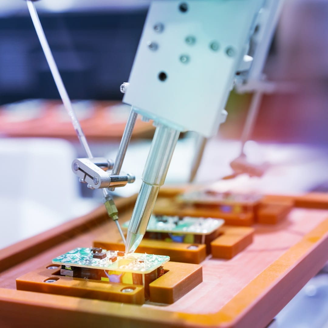
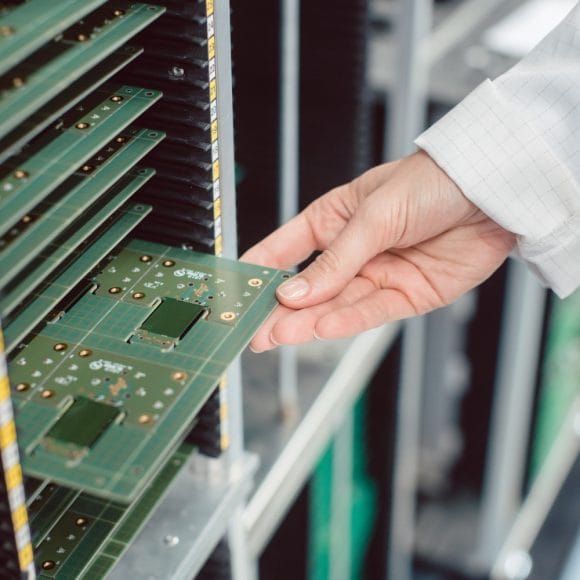
Custom Made Circuit Boards

We know PCBs are complex elements, and it can be difficult for hobbyists to design a working circuit. The first thing you will need is reliable software to create the blueprint of your PCB.

Then you can use many PCB design solutions, such as Eagle from Cadsoft Computer, which does an excellent job designing your PCB.

Prepare Schematic View

You have to prepare the schematic view to create your custom PCB. Access the component library that is present in your design software and places them onto the canvas.

Now you have to connect the pins with the lines that symbolize electrical connections in the software.

The same part number may confuse you as you will find several options.

The packages can include a surface-mounted chip or a Dual-in-line box (DIP). If you are a hobbyist or have a DIY project, it makes sense to go for significant and noticeable system-in-packages (SIP) or DIPs.

You can find them quickly, and hobby outlets are far more friendly when selling them than surface-mounted devices reserved for commercial applications.

The different packaging options can appear to be similar in the schematic view. However, things will appear differently when you switch to the layout view to begin your design.

You will need to provide the necessary ground and power signals apart from placing your interconnections and components; you can use the features such as GND, VDD, and VCC found in the Eagle library for the job.

Also, integrate the connectors on the board so that the ground and power can be employed. At this stage, you will also have any external device you want, such as a potentiometer or LEDs.

Your design needs to go through an electrical rule check or ERC after putting everything in place.

The test is crucial to ensure that there is no error present that will hamper your circuit board's functionality.

One common issue you face is wired that appear to be connected but are not real.

You can check for little dots in your Eagle software, representing the connection intersections of the wires.

Other problems may include ground and power signals that you forgot to connect.

So you should remember that the automated tests won't tell you if your board will carry out the desired action, but they can always validate the electrical properties of your design.

Schematic Diagram and Layout View

Access Board Layout View

After doing everything you need to do in the schematic view, you must move over to activate the board layout view.

Then you have made the switch, and you will find the components spread randomly in your Eagle software.

You will also see that the wires directly hook to the pins.

To make the picture a bit less messy, move the components until they make meaning.

For example, you can move the connectors to the edges so that things make sense.

You still have much work to do to produce the circuit board. So you have to dedicate signals to the layers but remember that the different layers present in the same layer should not touch each other.

The professional version of the Eagle solution comes with an auto-layout feature that can route the signals with a single click.

However, for users of the standard version, you must take things into their own hands. You may also find a design solution from your PCB manufacturer to take care of this step.

After you have laid down the signals, the time has come to run the DRC or the design check.

The check ensures that holes are drilled too close to a signal line.

It also notifies you if the traces are not at an optimum distance from each other or the edge of the board.

You can customize the rules, and sometimes your PCB vendor will offer a file that can be integrated with Eagle solution with specified DRC values. Then you can upload your design files if your project passes the DRC.

You should utilize a particular layer to add silkscreen lettering to the Top. The printing will help you know which component fits, presenting part numbers and outlines.

That enables you to avoid mistakes like placing a 100K resistor instead of a 1K one.

A Gerber file reveals the language of PCB design, and 3each board can have many files associated with them.

You will have a separate file for the specifications of the solder pads and different files for each layer. The drill files also carry the specifications of the drilling.

You can then upload the design to your manufacturer, who can use another program to present the final look of the layers, and you can also find out if the components are the right size to fit the holes.

With this, you have come to the end of creating a custom circuit board using design software. In the next chapter, we will explore how a manufacturer produces PCBs.

Schematic Diagram Design

How Printed Circuit Boards are Made

By now, you know how to custom design your PCB by reading the earlier chapter. The technology of PCB is complicated, and it needs to go through a multi-stage manufacturing process.

You also have to choose a manufacturer with all the high-precision equipment to bring your project to life.

We are going to discuss the PCB manufacturing process in brief just for you.

1. Making the Substrate

You can think of PCBs as sandwiches that come in multiple layers. The base material found in the middle is known as the substrate. Then the substrate material is responsible for giving width to the PCB.

You can view a PCB from the side angle and find that the thickest layer is the substrate.

Traditionally PCBs were made with fiberglass substrate, which is rigid. Nowadays, you can find flexible substrate material.

Many materials can be used, but one standard option uses special plastic for the substrate to tolerate high temperatures.

The material used to make the substrate is generally spread out. The manufacturer then dips or sprays it with epoxy resin.

Next, the material is rolled on to get the desired thickness, just like rolling your pie crust using a rolling pin.

The rollers stop rolling when the substrate reaches the desired thickness and passes to the next step, and the substrate is now placed in the oven to turn out solid and firm by curing it.

After completing this step, you have created the first layer of your PCB.

2. The Copper Layers

Depending on the purpose, PCBs have a simple or complex design. Apart from the foundation layer of the substrate, copper layers are another essential component.

The copper layers are essential to carry electricity throughout your PCB.

Your PCB cam comes with a single layer of copper applied to the Top or two layers on both sides of the substrate.

The PCB can also have numerous layers with other copper and substrate.

Some PCBs used in advanced devices or smartphones have more than 12 or 16 layers of copper.

Copper layers are much lesser in width than the substrate layers, and you won't have any electricity flowing through your circuit if they are absent.

The manufacturer can use a combination of different methods to bond the copper to the surface of the substrate.

Any standard methods involve heat, pressure, and adhesive so that the copper layers are firmly fixed on the substrate.

You can take your PCB for drilling after the copper has bonded with the substrate.

The PCB needs to transmit the charge to the right points from one layer to another layer in the board for your device to function.

You will have to create holes referred to as via for the cost to flow through.

The manufacturer has several options to drill holes in the PCB and use a CO2 laser, UV laser, or other equipment.

The accuracy and efficiency of the drilling machine determine the preciseness and complexity of the PCB.

You have to clean the holes of any debris or any material that might have been left behind after the process of drilling.

They can also be deburred to get additional material clinging to the PCB.

After that, the inner sides of the vias are coated with copper to carry the charge from one layer of the circuit board to another.

Next, you have to print the pattern of the circuit on the PCB. The manufacturer can deploy the copper accurately following the design to get the way on board.

Otherwise, they may apply copper to the entire board and remove it to etch out the circuit pattern.

The PCB may be subjected to an alkaline bath to remove unnecessary copper.

You must add other components, such as transistors, capacitors, or LEDs, on the PCB.

You can solder the pieces onto the PCB using a soldering iron. Before adding the features, the PCB is passed through a succession of electrical tests using a grid tester or flying probe to ensure no short circuits or open connections.

Your manufacturer may also use a machine to pump the parts to your PCB.

Copper Patterns
Copper Patterns

3. The Final Solder Mask

The metals that remain exposed on the circuit board can get damaged. The nature of copper is to rust, rendering your PCB useless.

You can adequately protect the copper plating and other components of the PCB by adding an extra protective layer on Top.

Generally, manufacturers use gold, nickel, or tin-lead to plate specific vulnerable parts of the PCB. To top it all, the manufacturer provides another layer on Top called the sold to ask.

The green color that you see in PCBs is due to the application of the solder mask layer; the solder mask also has some other functions apart from covering and protecting all the metal parts that don't need to form a connection with anything, the layer of solder mask also ensures that current flows to the right places following absolute paths.

Sometimes you may also find a layer of silkscreen on Top of the solder map used to carve labels on necessary parts.

After everything is done, the manufacturer will trim and shed off any extra material or unnecessary parts not required in your PCB.

Green Solder Mask
Green Solder Mask

Conclusion

The best for just you.

We have given you the gist, and we hope you liked and benefitted from this.

As promised from the early part of the article, we would ensure that you do not just get the right vendor but get the best from whatever it offers.

You wouldn't want to hesitate on this any longer, we are right behind you, and just a call will do! Contact us today and secure your interest in high-quality products.

Also, you can request a quotation, and in case you have troubling questions or suggestions, please feel free to contact us.


Back to top: Ultimate Guide to Custom PCBs

Special Offer: Get $100 off your order!

Claim your $100 discount by sending an inquiry today. Act now to save on your next project!
Please email [email protected] for details.

Related Post