


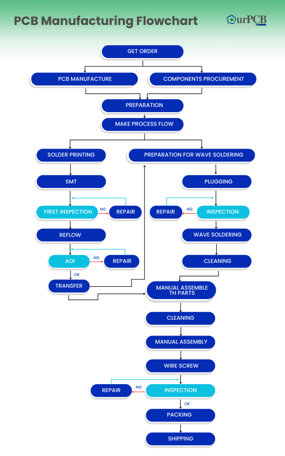

1. Design and Preparation
- OurPCB Technician analyzes a PCB design before approving it for production
- The process begins with PCB layout design, including defining electrical parameters, stack design, and component placement.
- Once finalized, essential design files (Gerber, Centroid, BOM, Pick-and-Place, NC Drill) are submitted for manufacturing.
- DFM (Design for Manufacturing) & DFA (Design for Assembly) checks ensure manufacturability by reviewing footprint design, component placement, solder mask clearances, and panelization.
- These checks help minimize defects, saving time and cost.
2. Component Sourcing and Procurement
- Components are sourced using the BOM and secured from in-house inventory or reliable suppliers (Avnet, Arrow, Future Electronics).
- Customers can supply their own components or have them shipped directly to the assembly plant.
3. PCB Fabrication
- Fabrication Steps: Printing PCB layout, etching, stack creation, hole drilling/plating, solder masking, silkscreen printing, and surface finishing.
- Rapid Prototyping Methods:
- Using simplified design rules.
- Prioritizing functional validation.
- Using simulated components.
- Running parallel prototype revisions.
- Multilayer boards require multiple etching/lamination cycles and additional inspection/testing for quality control.
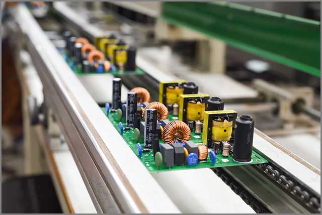
4. PCB Assembly (SMT & Through-Hole)
- SMT Process:
- Solder paste applied via stencil.
- Components placed using pick-and-place machines.
- Reflow oven fuses components (210–250°C for lead-free solder).
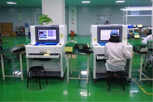
- Inspection & testing (AOI, X-ray, Flying Probe, Bed of Nails).
- Through-Hole Assembly:
- Automated insertion mount machines insert components.
- Wave soldering ensures solid connections.
- Final testing & functional checks follow, ensuring assembly accuracy before shipment.
5. PCB Testing & Quality Assurance
Testing Methods Include:
- In-Circuit Testing (ICT): Automated testing via spring-loaded pins.
- Flying Probe Testing: Precision mobile probes check connectivity.
- Burn-in Testing: Extreme stress tests for reliability.
- Functional Testing: Simulates real-world operational conditions.
- Other tests include aging, fatigue, and environmental stress testing.
6. Packaging & Shipping
- Prototype boards are securely packaged in antistatic bags with ziplock or vacuum sealing and desiccant packets for moisture control.
- Customers can choose between expedited or standard shipping based on urgency and cost preferences.

We handle everything from parts sourcing to final assembly, providing a hassle-free experience that ensures top-quality boards every time.
Whether you need a few prototypes or large-volume batches, our flexible assembly services adapt to your project’s scope and timeline.
Stay environmentally responsible with our compliant assembly processes, offering RoHS and lead-free options for safe, reliable builds.
No matter the complexity, we can assemble boards of all configurations—single-layer, multi-layer, or a mix—to match your exact specifications.
From one-off prototypes to bulk orders, we accommodate projects of all sizes without compromising on quality or turnaround time.
Join our growing community of satisfied clients who rely on our dependable assembly expertise and dedicated customer support.
Mon-Fri: 24 hours,
Sat: 9am-6pm, GMT+8
Reach us at
sales@ourpcb.net
24 hours online
+86-199-30589219
Mon-Fri: 24 hours,
Sat: 9am-6pm, GMT+8
Order options
Expedited prototypes with priority scheduling and full DFM review.
Accelerated bridge production with IPC Class 2/3 compliance.
Fast-turn high-volume manufacturing with automated inline testing.
★ What customers say
Third reorder of quick-turn PCB assemblies from OurPCB — consistent every time.
Turnaround on our quick-turn PCB assemblies order beat the quoted lead time by several days.
Great value on the quick-turn PCB assemblies for the quality we received.
Build quality on the quick-turn PCB assemblies was excellent; every unit passed our incoming inspection.
The quick-turn PCB assemblies arrived well-packed with full test reports included.
Easy to reach and proactive on status for our quick-turn PCB assemblies.

