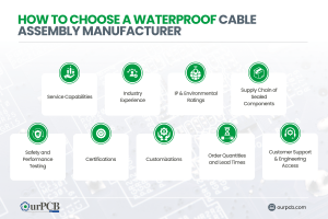
Top 8 Waterproof Cable Assembly Manufacturers
Waterproof cable assemblies have to do more than just “keep water out.” For outdoor, marine, industrial washdown, and transportation platforms, assemblies are expected to survive

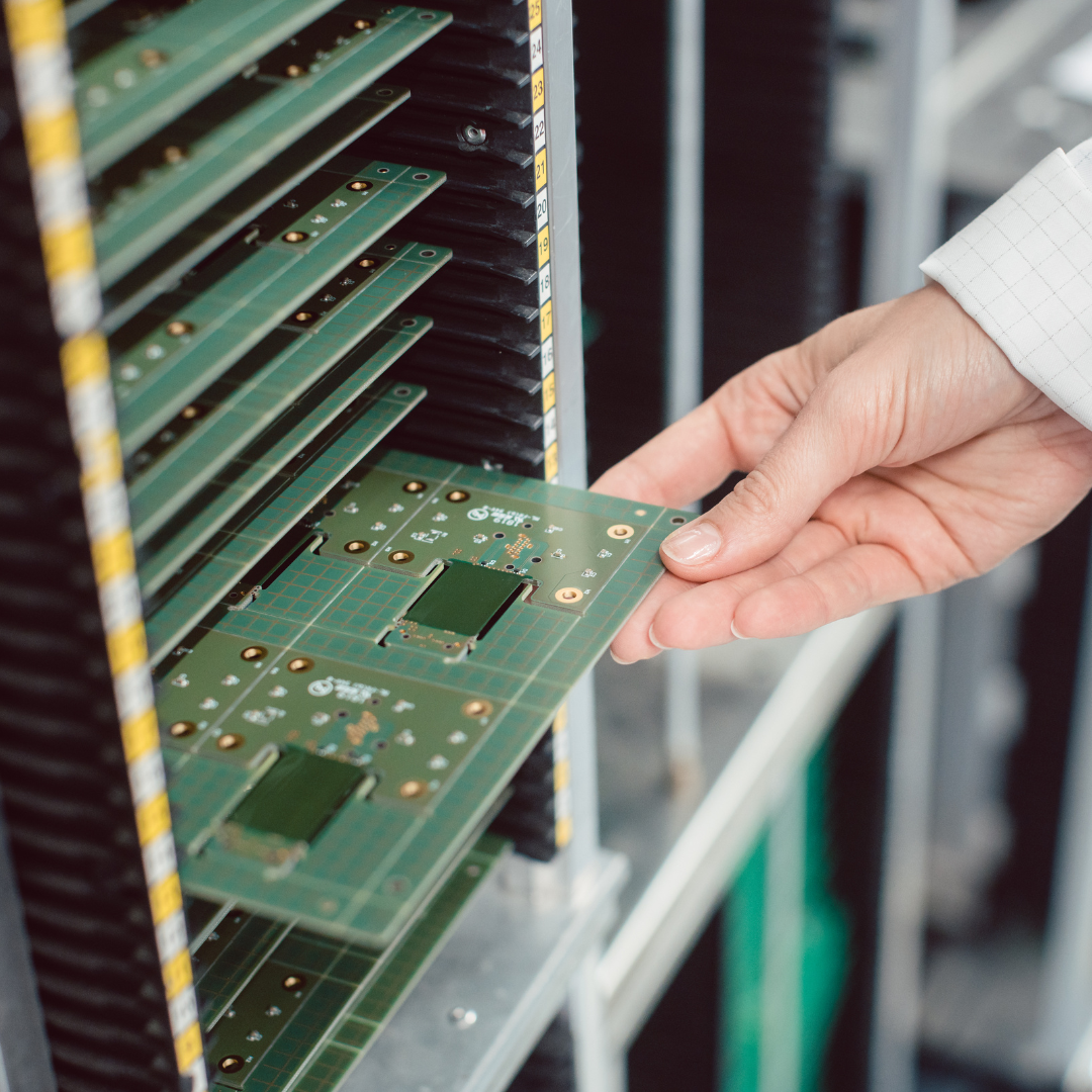
A 4 layer PCB stack-up is a circuit board with four conductive layers. It offers a balance of complexity and cost-effectiveness for many electronic designs. OurPCB specializes in manufacturing high-quality 4 layer PCBs for various industries and applications.


The fabrication of 4 layer PCBs starts with core material selection. We use FR-4 or high-frequency laminates based on your needs. The process involves precise layering of copper, prepreg, and core materials. We apply photoresist, expose, and etch the circuit patterns on each layer.
After etching, we laminate the layers together under heat and pressure. This creates a solid board structure. We then drill holes, plate them, and add solder mask and silkscreen. Our advanced equipment ensures accurate alignment and consistent quality throughout production.


OurPCB offers expert 4 layer PCB manufacturing services. We combine cutting-edge technology with years of industry experience. Our team is committed to delivering high-quality boards that meet your exact specifications.

A 4 layer PCB stack-up offers a good balance of performance and cost. It’s suitable for many electronic designs that need more complexity than 2 layer boards. Here’s why you might choose a 4 layer PCB:

OurPCB offers comprehensive PCB assembly services to complement our fabrication capabilities. We handle projects of all sizes and complexities. Our assembly services ensure your boards are ready for immediate use upon delivery.
We use advanced Surface Mount Technology for high-density, compact designs. Our SMT lines handle a wide range of component sizes and types. This process is ideal for modern, space-constrained electronic products.
We adapt to your needs. You can provide components, or we can source them for you. Our turnkey service covers everything from part procurement to final assembly. This flexibility helps streamline your production process.
Every project is unique. We tailor our assembly process to your specific requirements. Our team works closely with you to understand and implement your design intent. This ensures the final product meets your exact needs.
Time is often critical in electronics development. We offer fast turnaround options without sacrificing quality. Our efficient processes and dedicated teams make quick deliveries possible. This helps you meet tight project deadlines.
For high-reliability applications, we offer IPC Class 3 assembly. This standard is crucial for aerospace, medical, and other critical industries. Our strict quality controls ensure these demanding requirements are always met.
We have expertise in assembling all types of IC packages. This includes BGAs, QFNs, and other complex components. Our advanced equipment and skilled technicians ensure precise placement and reliable connections.
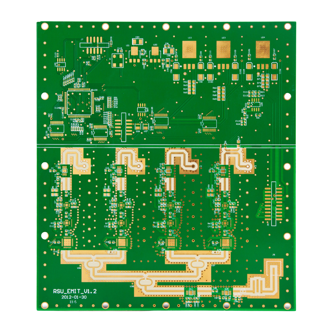
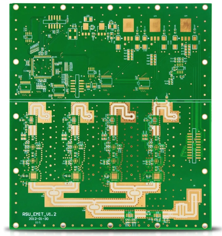
OurPCB’s technical capabilities cover a wide range of 4 layer PCB specifications. We can produce boards with thicknesses from 0.1mm to 10mm. Our minimum trace width and spacing is 2.5/2.5mil. We offer various surface finishes including HASL, ENIG, and immersion tin. Our standard FR-4 material is suitable for most applications, but we also work with high-frequency laminates. We can handle board sizes up to 22.5 x 47.2 inch.
Mon-Fri: 24 hours,
Sat: 9am-6pm, GMT+8
Reach us at
[email protected]
24 hours online
+86-199-30589219
Mon-Fri: 24 hours,
Sat: 9am-6pm, GMT+8
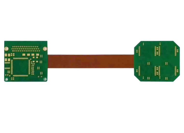
The four layers of PCB stack-up are the top layer, inner layers, and bottom layer. A typical 4 layer PCB board includes signal, power, and ground planes for optimized performance. The 4 layer PCB power plane and 4 layer PCB ground plane ensure stable voltage and signal integrity. This multilayer PCB design improves high-speed capabilities and minimizes interconnect issues.
The 4 layer board fabrication process starts with PCB production and preparing copper layers. Inner layers are etched with copper foil for circuits, followed by lamination with dielectric. Vias connect internal layers to outer layers, ensuring reliable interconnect paths. Finally, the board thickness is refined for optimal 4-layer PCB output quality.
4 layer PCB design rules focus on 4 layer PCB design for manufacturability guidelines to prevent errors. Proper 4 layer PCB layout includes HDI techniques and careful placement of vias. The 4 layer PCB tutorial emphasizes high-frequency management and minimizing crosstalk between layers. Adhering to a PCB stack-up guide ensures that the layers of the PCB function efficiently.
Waterproof cable assemblies have to do more than just “keep water out.” For outdoor, marine, industrial washdown, and transportation platforms, assemblies are expected to survive
Aerospace cable assembly manufacturers work under standards such as AS9100, ISO 9001, and RTCA/DO-160, and many also maintain ITAR registration to support flight-critical and space-qualified

When considering the best places for manufacturing data cables, China immediately comes to mind. It’s no surprise either — the country has rapidly ascended in
Finding the right wiring harness manufacturer for your vintage ride can be a real headache. Those beautiful old machines need special wiring that looks period-correct
Would your car be able to run without wire harnesses? Not a chance. Wire harnesses connect all the electrical parts together. No harness means no
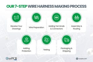
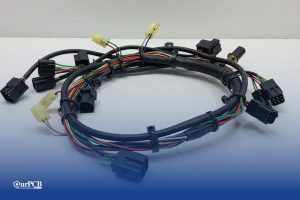
Making wire harnesses isn’t complicated. At OurPCB, we create custom wire harnesses for an expansive range of industries every day. While it’s a complicated process,
We use cookies to improve your browsing experience, which may include personal information. By clicking "Agree," you accept our Privacy Policy and cookie use. You can change your cookie settings in your browser anytime.
Agree Chat With Us
 Free Quote