
Who are the Top 6 Data Cable Manufacturers in China?
When considering the best places for manufacturing data cables, China immediately comes to mind. It’s no surprise either — the country has rapidly ascended in

OurPCB is a leading 12 layer PCB manufacturer and supplier. We specialize in creating high-quality, multi-layer printed circuit boards for complex electronic devices. Our team uses advanced technology and strict quality control to ensure reliable performance. With years of experience, OurPCB delivers custom solutions tailored to your specific needs.


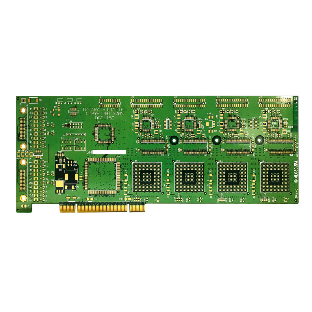

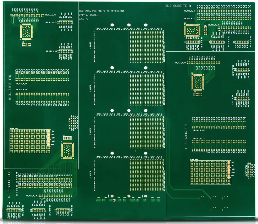
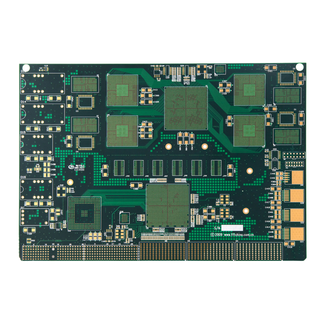
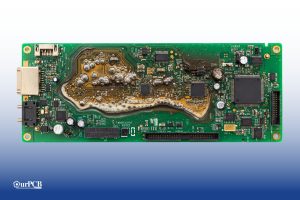
12 layer PCB stack-up manufacturers produce complex circuit boards with multiple conductive layers. These boards are essential for high-density electronic devices that require advanced functionality. Manufacturers like OurPCB use specialized equipment and techniques to create precise layer alignments and connections.
The production process involves careful planning of the PCB stackup design. This includes determining the placement of signal layers, power planes, and ground planes. Manufacturers must also consider factors like impedance control and signal integrity. Quality control is crucial throughout the fabrication process to ensure the final product meets strict industry standards.


Partnering with OurPCB as your 12 layer circuit board supplier offers numerous advantages. We combine technical expertise with customer-focused service to deliver top-quality PCBs. Here are the key benefits of choosing OurPCB:

A 12 layer PCB stackup offers significant advantages for complex electronic designs. It provides more routing options and better signal management. Here’s why you might opt for a 12 layer PCB:

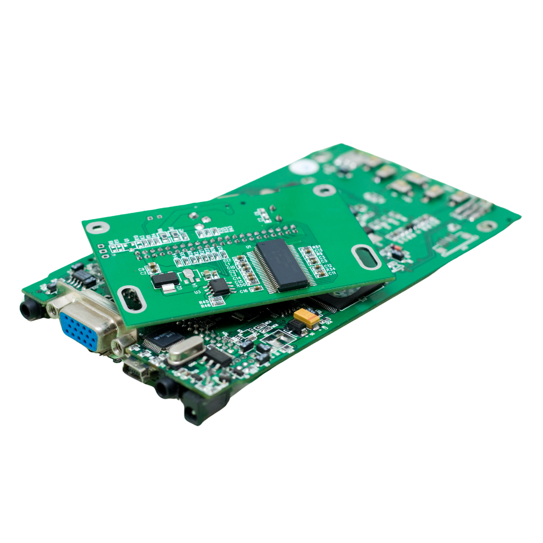
OurPCB offers comprehensive PCB assembly services to complement our fabrication capabilities. We handle projects of various sizes and complexities. Our assembly services include:
We use Surface Mount Technology for high-density, compact PCB assemblies. Our SMT process ensures precise component placement and reliable solder connections.
We accommodate both customer-supplied components and full turnkey solutions. Our turnkey service covers component sourcing, assembly, and final delivery.
Our team works closely with clients to deliver tailored assembly solutions. We adapt our processes to meet unique design requirements and specifications.
We offer fast turnaround times without compromising quality. Our efficient processes enable rapid prototyping and small-batch production.
We adhere to strict IPC Class 3 standards for high-reliability applications. This service is ideal for aerospace, medical, and other critical industries.
We have expertise in assembling various IC package types. This includes BGA, POP, CGA, QFN, DFN, and CSP components.
OurPCB possesses advanced technical capabilities for 12 layer PCB fabrication. We use high-precision drilling and lamination equipment to achieve tight tolerances. Our facility can produce boards with minimum trace widths of 2.5 mil and minimum via sizes of 0.1 mm. We offer a range of surface finishes, including ENIG, HASL, and immersion silver. Our in-house testing equipment ensures every board meets strict quality and performance standards.
Mon-Fri: 24 hours,
Sat: 9am-6pm, GMT+8
Reach us at
[email protected]
24 hours online
+86-199-30589219
Mon-Fri: 24 hours,
Sat: 9am-6pm, GMT+8
A 12 layer PCB board typically has a board thickness of 1.6 mm to 2.4 mm. This thickness depends on the laminate, prepreg, and copper layer configuration. 12 layer PCB fabrication suppliers ensure precise control of these materials. Consistent thickness is crucial for reliability and durability in multilayer PCB design.
Yes, the 12-layer PCB stack-up can include a heat sink for better thermal management. HDI techniques and vias help dissipate heat efficiently through the outer layer of the PCB. A proper 12-layer PCB stack-up design integrates a substrate with high thermal conductivity. This approach enhances the manufacturing process and extends the board’s durability.
12-layer PCBs are used in applications requiring high reliability and complex circuitry. They are common in telecommunications, aerospace, and advanced computing systems. The multilayer PCB design supports HDI features for compact and efficient interconnects. Choosing a reliable PCB supplier ensures high-quality 12 layer PCBs with effective dielectric properties.
When considering the best places for manufacturing data cables, China immediately comes to mind. It’s no surprise either — the country has rapidly ascended in
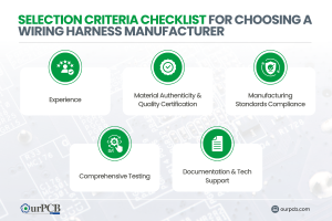
Finding the right wiring harness manufacturer for your vintage ride can be a real headache. Those beautiful old machines need special wiring that looks period-correct
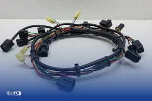
Would your car be able to run without wire harnesses? Not a chance. Wire harnesses connect all the electrical parts together. No harness means no
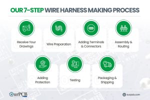
Making wire harnesses isn’t complicated. At OurPCB, we create custom wire harnesses for an expansive range of industries every day. While it’s a complicated process,

Prototype cable assemblies are the very important place in between PCB design ideas and interconnects. OurPCB brings prototype assemblies with PCB solutions to your tables.
PCB thermal management prevents component overheating through strategic heat transfer techniques. Without proper thermal control, electronics are at risk of electronic failures through weakened solder
We use cookies to improve your browsing experience, which may include personal information. By clicking "Agree," you accept our Privacy Policy and cookie use. You can change your cookie settings in your browser anytime.
Agree
 Chat With Us
 Free Quote