


Pre-Assembly BOM Validation for RoHS Compatibility
Each job is reviewed by engineering to verify lead-free component status and solderability.
We check BOM part numbers against plating libraries and confirm that all component finishes, matte tin, SnCu, or SnAg, are compatible with lead-free solder paste alloys.
MSL-3 and higher components are baked for 24 to 48 hours at 125 °C per J-STD-033 before placement.
Internal Control of Lead-Free Surface Finishes
We apply ENIG (2 to 5 µin Au over 120 to 240 µin Ni), lead-free HASL, OSP, and Immersion Silver in-house. Surface finishes are selected based on alloy wetting compatibility, shelf life, and pad geometry.
All finish lines are RoHS-aligned, and finish data is included with every RoHS-compliant PCB order.
Thermally Rated Stackups for 260 °C Reflow
Stocked materials include FR408HR, IS420, and G200, each rated for ≥260 °C lead-free reflow.
These laminates pass T288 delamination testing at 288 °C with hold times over 6 minutes and Td ≥340 °C.
Stackups are modeled to maintain resin-glass stability across two or more lead-free assembly cycles, preventing copper barrel fatigue or dielectric deformation.
RoHS Documentation Delivered Per Job
All assemblies are delivered with solder paste lot IDs, reflow validation charts, finish certs, and laminate origin.
This RoHS package is supplied by default with every lead free PCB assembly, eliminating the need for post-shipment document requests and accelerating downstream compliance, inspection, or integration for export-regulated applications.
All consigned PCB kits are assigned a unique internal tracking ID at intake. Components are unpacked, sorted by feeder compatibility (tray, tube, tape), and checked against the BOM line-by-line.
Discrepancies in part number, reel labeling, or quantity shortfall trigger a hold and customer notification before any line setup is authorized.
Moisture-sensitive components are scanned for MSL classification and timeout. Floor-exposed parts are queued for bake-out and resealing before feeder prep.
Kits are then moved into a staging buffer with recorded timestamps, ready for scheduled job release into SMT or PTH lanes within a 24-hour window to avoid MSL re-exposure.
Feeder lanes are assigned based on component pick frequency, rotation offset, and machine head type (high-speed vs. multi-function).
Job setup includes vision system calibration, feeder load sequence, and nozzle selection to match the footprint.
For cut tape or partial reels, feeder splicing or leader creation with cover tape is performed in-line.
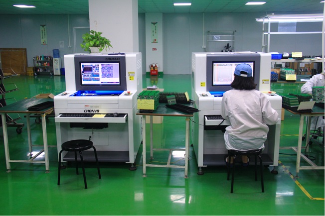
Boards flagged for BGA, PoP, or QFN automatically route to X-ray before post-reflow AOI.
Inspection sequence follows preassigned logic: X-ray → AOI → functional test, with exception routing for manual visual review if solder bridges or lifted leads are detected.
Final pass/fail disposition is recorded against the internal build traveler before packaging.
Once released to production, boards follow the programmed sequence of stencil printing, SMT placement, and thermal profile reflow based on solder type and component density.
For double-sided builds, bottom-side SMT is supported with low-tack adhesive or pallet fixturing. If mixed with PTH, boards are transferred to selective soldering or manual insertion before final reflow or wave pass.


OurPCB executes lead-free PCB assembly through a calibrated, fully documented process built around RoHS compliance, alloy-specific soldering, and internal finish control.
All steps, from stencil printing to final inspection, are performed in-house using isolated tooling, nitrogen-assisted ovens, and standards-based validation under IPC-A-610 Class 2 or Class 3 requirements.

Solder Paste Printing and Inspection
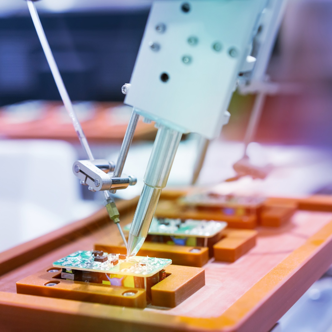
Lead-free solder paste uses stainless steel stencils and precision screen printers with ±15 µm alignment accuracy.
Paste type matches surface finish, component pitch, and board layout. SPI (Solder Paste Inspection) systems verify deposit height, volume, and coverage within ±5% tolerance across critical pads.

Component Placement with Alloy-Matched Profiles
SAC305 or SnCu solder alloys are selected based on BOM compatibility and finish type.
Components use high-speed pick-and-place platforms with optical centering and down-looking vision systems. BGA, µBGA, and BTC devices are aligned within ±25 µm before reflow.

Nitrogen Reflow Soldering
Boards are reflowed on nitrogen-controlled 10-zone ovens. Thermal profiles are tuned by layer count, copper plane mass, and laminate Tg.
SAC-class pastes are processed at peak temperatures of 245 to 250 °C, with dwell times of 10 to 15 seconds above 217 °C. Profiling is verified with thermocouples and job-specific coupons.

Selective Wave and Manual Soldering for PTH
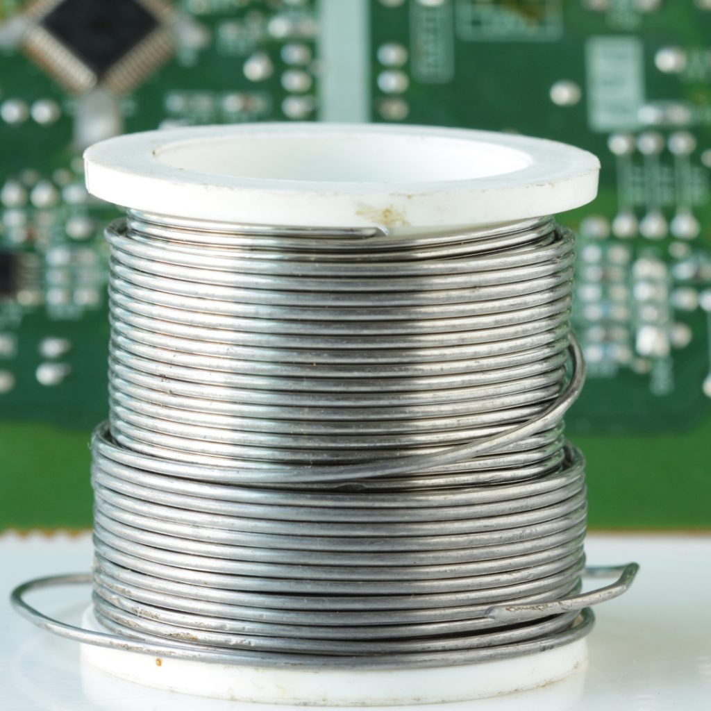
For mixed-technology boards, through-hole components are soldered using lead-free wave systems with SAC305 or SnCuNi solder.
Flux application, dwell time, and conveyor speed are calibrated to board thickness and copper distribution.
Manual soldering stations use RoHS-compliant solder wire and temperature-controlled tips under ESD protection.

Post-Reflow Cleaning and Conformal Coating
Assemblies using water-soluble or no-clean flux undergo process-specific cleaning in batch or inline systems.
Cleaning agents are RoHS-certified and alloy-compatible.
Boards requiring coating receive optional acrylic or silicone-based conformal films applied by spray, dip, or selective coating with UV inspection.

Final Inspection and Documentation
All lead-free PCB assemblies undergo 2D AOI and 5-axis X-ray (≤15 µm resolution) for BGA and BTC solder joint validation. Functional or ICT tests are applied where specified.
Reflow and inspection data are archived per job and included with the RoHS compliance package for each shipment.
What Surface Finishes are Available for Lead-Free PCB Assembly?
OurPCB offers multiple surface finish options that meet RoHS and lead-free assembly requirements, each selected based on solder paste compatibility, pad geometry, and wetting behavior under high-temperature reflow.
All finishes are applied in-house and tracked by job number, thickness, and plating date as part of our lead-free PCB assembly documentation package.
Electroless Nickel Immersion Gold (ENIG)
ENIG is applied with 120 to 240 µin of nickel and 2 to 5 µin of immersion gold, following IPC-4552A. Nickel provides diffusion resistance while gold preserves solderability under high-heat reflow.
This finish pairs well with SAC305 lead-free solder paste, offering flatness critical for lead-free PCB assembly involving BGA, QFN, or µBGA layouts. ENIG supports multiple 260 °C reflow cycles without oxidation and maintains solder joint planarity for high-density SMT.
Lead-Free Hot Air Solder Leveling (HASL)
Lead-free HASL finishes are applied with SnCu or SnNi solder at 260 to 270 °C, then leveled with high-velocity air knives. Thickness ranges from 100 to 500 µin, measured against IPC-6012 standards.
This finish supports lead-free PCB manufacturing using through-hole or mixed-technology components and is compatible with SAC-class and SnCuNi lead-free solder. It offers excellent solder wetting and mechanical robustness but is unsuitable for 0.4 mm or finer pitch components due to surface unevenness.
Organic Solderability Preservative (OSP)
OSP coatings are deposited via horizontal conveyor systems to a controlled film thickness of 0.2 to 0.5 µm. The organic layer inhibits copper oxidation before soldering and is removed during the first reflow.
OSP is RoHS compliant and optimized for single-pass lead-free reflow using SAC305 solder paste. It is commonly used in high-yield SMT lead-free PCB assembly, but not recommended for boards requiring multiple thermal cycles or extended shelf life beyond 6 months.
Immersion Silver and Immersion Tin
Immersion Silver coatings are applied to 5 to 12 µin thickness, offering low contact resistance and substantial wetting for SAC-class lead-free solder alloys. Immersion Tin creates a SnCu intermetallic directly at the copper interface, applied to a 30 to 50 µin thickness.
Both finishes are RoHS compliant and suitable for medium-volume lead-free PCB assemblies requiring flat pads and reliable first-pass yield. Silver is preferred for multiple reflow cycles; Tin is selected when oxide prevention and surface planarity are the priority.
What Materials do we use for RoHS-Compliant PCB Manufacturing?
All materials used in lead-free PCB manufacturing are certified to meet the thresholds outlined in the RoHS directive 2015/863, with no more than 0.1% by weight of restricted substances such as lead, mercury, or hexavalent chromium.
Every PCB order requiring lead-free processing is matched to compliant stackups and solder alloys to reduce the risk of failed inspection or restricted shipment due to banned lead content.
High-Tg Laminates for Lead-Free Assembly Cycles
We stock UL-certified base materials including FR408HR, IS420, and G200 for high-temperature lead-free reflow. These laminates support 260 °C peak temperature profiles and meet IPC-TM-650 Method 2.4.24.1 for delamination time (T288) exceeding 6 minutes.
Dielectric properties (Dk 4.1 to 4.3, Df ≤ 0.008) remain stable through multiple reflow cycles, and each stackup is validated for copper thickness, press-out, and expansion behavior.
These lead-free PCB designs support thermal reliability without degradation in dimensional tolerance, impedance, or resin-glass bond strength across the full assembly cycle.
Lead-Free Compatible Solder Alloys
Solder alloys used in our facility include SAC305, SnCuNi, and low-Ag high-reliability blends, selected through internal solder alloy selection guidelines.
These alloys form lead-free solder joints with controlled wetting angles, predictable intermetallic thickness (1 to 2 µm), and reduced crack propagation under strain.
Each batch is certified for <1000 ppm impurities and <100 ppm lead use. Mechanical performance under shear and vibration is validated using JEDEC JESD22-B111.
These lead-free materials are part of our lead-free solutions portfolio applied across all Class 3 PCB manufacturing and assembly jobs.
Surface Finishes Matched to Paste and Alloy
ENIG, lead-free HASL, Immersion Silver, and OSP are applied in-house. Each lead-free surface finish is selected based on compatibility with component terminations, lead-free solder paste type, and board layout.
Immersion finishes are tested for shelf life stability, oxide layer thickness, and wetting behavior under SAC-class alloys. HASL coatings are evaluated for planar uniformity and solder mask dam clearance per IPC-6012.
These materials are used across PCB fabrication and assembly jobs requiring reflow consistency, press-fit durability, or fine-pitch pad coplanarity.
RoHS-Certified Components and Termination Finishes
All BOMs, including component body materials and terminal plating, are checked for RoHS conformity.
We validate each part as compliant with lead-free and RoHS standards and confirm plating compatibility across ENIG, SnCu, and SnAg finishes.
Components used in lead-free circuit board builds are verified for moisture sensitivity (MSL) and thermal exposure limits based on JEDEC J-STD-033.
This prevents exposure to lead and ensures long-term solder joint reliability across fine-pitch ICs, BGA, and bottom-terminated devices on RoHS-compliant PCB builds.
What Testing and Certifications do Our Lead-Free PCBs Meet?
Turnkey PCB assembly is best when you want OurPCB to manage sourcing, while consignment gives you control over the components you supply. We recommend turnkey for fast lead times, stable BOMs, and minimal sourcing overhead.
Consignment PCB assembly is better when you need to protect proprietary parts, use pre-purchased inventory, or meet strict vendor requirements. Our team supports both models and helps you select the most efficient path based on supply chain control, traceability needs, and build complexity.

AOI and X-Ray Validation for Lead-Free Solder Joints
Our PCB Boards undergo 100% inspection using 12 to 15 µm automated optical inspection (AOI) and 5-axis X-ray imaging.
We identify defects, including insufficient solder, tombstoning, wetting imbalance, and head-in-pillow on BGAs or bottom-terminated components.
For X-ray-inspected assemblies, we scan for voiding <25% per IPC-7095D guidelines for lead-free solder joints, which ensures current-carrying capacity and reduces heat buildup within SAC-class intermetallic layers, and maintain image logs for all BGA nets and broadline distribution sourcing.
Solderability Testing and Ionic Contamination Control
We apply solderability tests per IPC-TM-650 Method 2.6.33 for surface finish wetting verification before placement. Ionic cleanliness is tested using resistivity of solvent extract (ROSE) to meet ≤1.56 µg NaCl/cm² for no-clean flux and ≤0.75 µg for water-soluble flux.
These procedures validate that the board is a compatible lead-free process suitable for high-density fine-pitch component mounting without surface oxidation or flux residue buildup.
Thermal Profile, Alloy Traceability, and MES Logging
Each lead-free PCB manufacturing job includes archived thermal profile logs from 10-zone nitrogen reflow ovens.
We record soak time, peak temperature, and dwell at liquidus using embedded K-type thermocouples and track solder paste lot number, alloy type, and date code per job traveler.
These controls are structured to prevent undocumented RoHS lead content or off-spec thermal excursions across long-run or repeat builds.
RoHS Compliance Certification and Product Labeling
Finished boards are labeled with RoHS compliance marks per RoHS directive 2015/863, and documentation includes full material declarations, solder alloy certification, and process conformance.
All RoHS-compliant PCB shipments include a C of C, RoHS declaration, and optional test coupon report.
Our process aligns with lead-free and RoHS standards for all regulated lead-free products, including medical, automotive, and telecom hardware, subject to global certification.
Mon-Fri: 24 hours,
Sat: 9am-6pm, GMT+8
Reach us at
[email protected]
24 hours online
+86-199-30589219
Mon-Fri: 24 hours,
Sat: 9am-6pm, GMT+8


