

Why Apple Manufactures in China (And What Hardware Startups Can Learn From Its Playbook)
When asked why Apple manufactures in China, ‘cheap labor’ is the facile answer. The more accurate one is supply chain engineering. A modern iPhone may
 5 Star Rating on
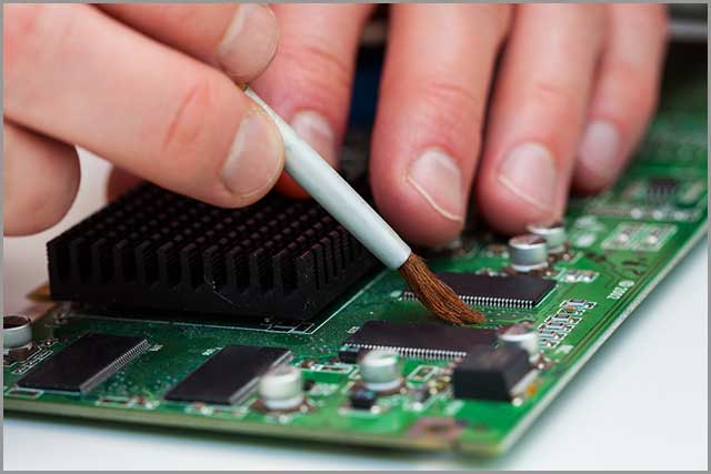
 OurPCB applies PCB conformal coating across medical, aerospace, industrial, and automotive electronics using brush, spray, dip, and vapor deposition.
Each coating layer increases dielectric strength, prevents current leakage, and extends the service life of mission-critical electronics.
We support all major coating types, including acrylic, epoxy, silicone, polyurethane, and parylene conformal coatings.
✅ ISO 9001, IATF 16949, and IPC-A-610 Class 2 & 3 compliant.
✅ Robotic spray, selective masking, and UV inspection.
✅ Turnkey PCB conformal coating services aligned with full assembly.


Choosing the right PCB manufacturer for EV chargers means more than just hitting specifications; it’s about consistent quality, fast lead times, and a partner who understands the regulatory and reliability pressures of electric vehicle infrastructure. OurPCB delivers that foundation across every layer of design and production.


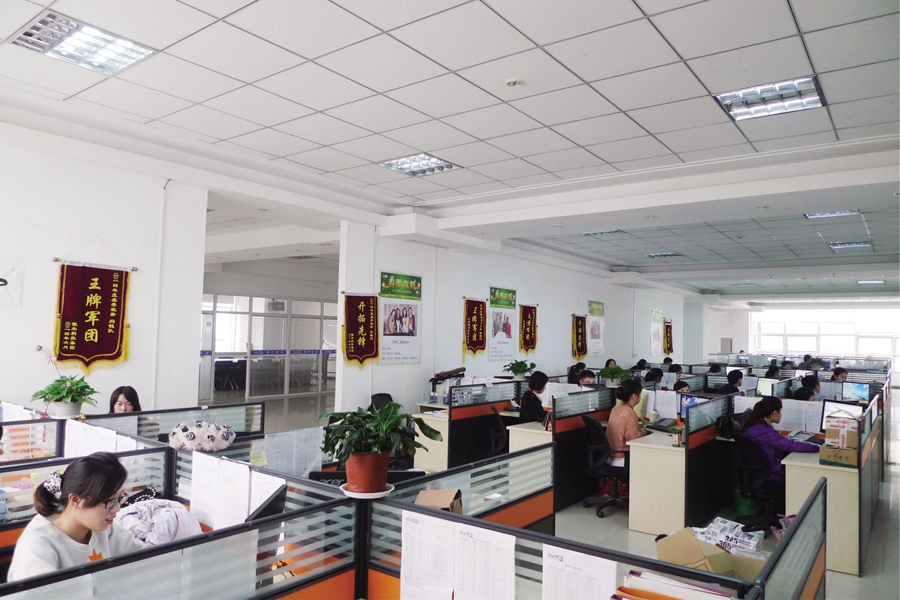
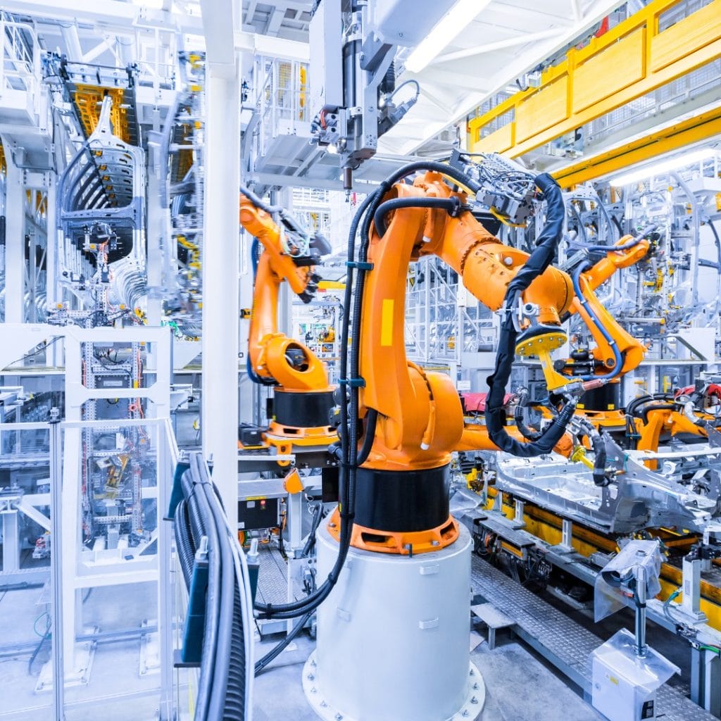
OurPCB operates two fully equipped manufacturing sites in China, each covering over 10,000 square meters of production space.
These facilities are built to support high-volume EV charger PCB assembly across SMT, THT, and hybrid processes. Both sites are vertically integrated, allowing for seamless control over fabrication, assembly, testing, and final packaging.
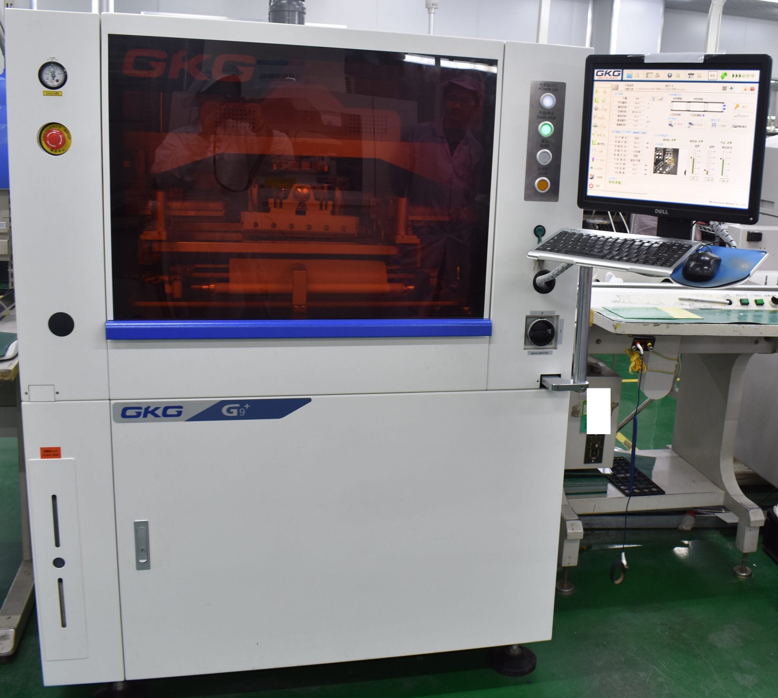
Production lines are outfitted with advanced equipment, including solder paste printers, reflow ovens, AOI systems, BGA rework stations, and ICT testers. Dedicated zones are maintained for nitrogen reflow, X-ray inspection, and conformal coating to support high-voltage PCB applications in EV charging systems.

OurPCB manufactures EV charger PCBs in facilities certified to ISO 9001:2015 and IATF 16949:2016, meeting the requirements for automotive and high-reliability electronics.
We build to IPC-A-610 Class 2 by default, with full capability for Class 3 when higher durability or safety margins are required.
Our engineering workflows also support PCB assembly projects targeting IEC 61851 and ISO 15118, a smart charging protocol enabling EV authentication via the control pilot line.

Since 2007, OurPCB has delivered precision PCB assembly services to over 3,000 customers across 40 countries.
Our client base spans electric vehicle manufacturers, automotive Tier 1 suppliers, charging infrastructure developers, and industrial energy OEMs. This depth of experience enables us to meet the performance, cost, and compliance expectations of global EV programs.
We support both prototype and mass production needs, with structured NPI workflows and repeatable process controls.
Clients rely on our technical stability, fast response times, and consistent output across multilayer charger boards, control PCBs, and power regulation modules.

OurPCB provides full engineering support to streamline EV charger PCB design and accelerate production readiness.
Our in-house team reviews all Gerber files, BOMs, and stack-ups for manufacturability, focusing on high-voltage isolation, trace current capacity, and controlled impedance requirements.
We assist with impedance matching, conductor width calculations, and interlayer clearance analysis to meet the demands of AC and DC charger designs.
For complex builds, we offer design feedback for structures, thermal reliefs, and pad geometries, along with guidance on compliance with IPC, IEC, and regional safety standards.

OurPCB sources all components for EV charger PCB assemblies from authorized global distributors, including Mouser, Digi-Key, Future Electronics, and WPG.
We manage lifecycle status, lead time risk, and cross-referencing to ensure stable sourcing for automotive-grade components such as SiC MOSFETs, gate drivers, current sensors, and power supply ICs.
All incoming materials are subject to ESD-safe handling, lot-level inspection, and barcode tracking throughout the assembly process.

OurPCB supports rapid program timelines with fast and accurate quoting for EV charger PCB builds.
Standard quotes for bare PCB fabrication are delivered within 8 working hours, while full turnkey PCBA quotes with component sourcing are provided within 48 hours.
Our staff works directly with engineers and procurement teams to resolve DFM questions, confirm delivery schedules, and manage revisions across global time zones.
OurPCB applies conformal coatings as part of a tightly controlled in-house process aligned with IPC, ISO, and IATF standards. Our equipment, QA systems, and trained operators support both low- and high-volume builds across all standard coating chemistries. All work is integrated with our broader PCB manufacturing and assembly workflows to maintain consistency from soldering through final coating inspection.

Our PCB conformal coating services are housed within two 10,000 m² production plants in Shenzhen and Shijiazhuang, each certified to ISO 9001:2015 and IATF 16949:2016.
Coating processes comply with IPC-CC-830B and support MIL-I-46058C and UL 746E classifications.
For aerospace, space, and medical applications, we meet ASTM E595 low outgassing standards, maintain ISO 13485 process control, and document coating batches for FDA Device Master File submission.
Environmental controls in coating areas include HEPA filtration, controlled humidity (<55%), and FOD-restricted zones.
Each coated board is inspected under UV blacklight for uniformity, edge bleed, voids, and incomplete masking.
Coating thickness is measured with contact meters to confirm target film builds between 25 and 100 μm, depending on the specified insulation requirement.
AOI is used for selective spray zones and keep-out regions. Post-cure inspection includes adhesion verification (tape pull method per IPC-TM-650) and dielectric withstand testing when specified.
All QA results are stored with time-stamped traceability and operator records.
Coating technicians are IPC-A-610 and IPC-CC-830 trained, with documented proficiency in masking, selective spray operation, and rework methods.
Operators are required to complete qualification panels with defined edge resolution, material compatibility, and rework simulation.
Engineering support includes reviewing coating flow maps, curing window validation for materials like epoxy resin and silicone resins, and defining coverage zones for assemblies with exposed test pads, heat sinks, or pressure sensors.
Our production lines accommodate volumes from single prototype boards to panelized arrays up to 18″ x 22″, with fixture-based masking and inline handling.
Coating programs can be configured with process staging: pre-cleaning, masking, coating, curing, and inspection.
We support projects requiring single-chemistry or dual-chemistry coating systems (e.g., dip conformal coating plus selective spray conformal coating).
Batch ID, lot number, coating method, and cure conditions are tracked digitally for each job, and material changes are logged under engineering change control.
At OurPCB, we remove no-clean flux during the PCBA cleaning process to prevent insulation resistance loss, support coating adhesion, and avoid inspection rejection in Class 2 and 3 assemblies.
Although low-solid no-clean flux is engineered to remain on the board, its residue absorbs moisture, lowers surface resistivity, and disrupts conformal coating uniformity, especially near component edges or mask-defined pads.
Our PCBA cleaning procedures are based on flux type, component density, and coating thickness requirements, and are qualified using ionic cleanliness testing, white residue detection, and surface preparation metrics that ensure coating and inspection compliance.
We remove no-clean flux residue because its remaining solids form hygroscopic films with ionic content capable of enabling leakage currents under bias. These residues often contain halide activators or rosin derivatives that, in humid environments, allow ionic mobility as low as 10⁸ Ω insulation resistance across narrow conductor spacing.
On high-density printed circuit board assemblies, especially those with ≤0.3 mm pitch, this can lead to dendritic growth, moisture-induced tracking, and eventual open or short failures. In Class 3 applications, even visually benign residues violate IPC J-STD-001 Section 8.3.1, prohibiting any visible residue under conformal coating.
Removing these residues is required to maintain dielectric performance and prevent latent field degradation.
Our cleaning strategy depends on the flux chemistry and board design. For fully assembled SMT boards, we use vapor degreasing with HFE-72DA or Vertrel XF, which condense at 55 °C – 65 °C onto the PCBA surface, dissolve polar and non-polar residues, and evaporate without leaving water or exposing components to immersion.
In rework areas or where selective cleaning is required, we use Decotron T383 or high-purity IPA with aerosol precision nozzles to rinse solder ball traps and low-solids residue from around pads.
The process is followed by 30 psi filtered air drying or vacuum-assisted drying to prevent water adsorption beneath packages. Surface prep is validated using surface insulation resistance (SIR) measurements, ionic testing (<1.56 µg/cm² NaCl equivalent), and UV light to detect fluorescence from missed residues.
Removing flux residue allows for consistent conformal coating flow and edge adhesion, especially in boards using urethane or acrylic coatings. Cleaned surfaces increase surface energy, improving film wetting and eliminating common defects like dewetting, bridging, or edge lift.
Coating adhesion strength improves from 1.2 N/mm (on flux-contaminated surfaces) to over 2.5 N/mm on properly cleaned copper and solder mask regions, reducing delamination risk during thermal cycling. In addition, a clean PCB surface ensures that automated optical inspection (AOI), UV inspection, or manual visual checks can accurately detect voids, bubbles, or skipped areas.
For applications in automotive ECUs, implantable medical devices, or high-speed digital RF systems, surface cleanliness before coating directly correlates to long-term device reliability in harsh conditions.
OurPCB provides precision PCB conformal coating services integrated directly into the PCBA production line. We apply high-performance coating materials using selective, scalable, and standards-driven processes that match the specific electrical, thermal, and chemical protection requirements of each application. All coating operations are handled in-house with automated equipment and certified staff.
We support all IPC-CC-830 coating classes, including AR (acrylic), SR (silicone), UR (polyurethane), ER (epoxy), and XY (parylene).
Each type of coating is chosen based on operating temperature, dielectric strength, solvent resistance, and reworkability.
For example, acrylic offers 90 to 100 kV/mm insulation and easy repair, while parylene conformal coatings form pinhole-free layers for precision analog protection and meet ASTM E595 outgassing specs.
We operate fully enclosed robotic spray systems with 3-axis selective heads, dip coating stations with vertical/horizontal immersion control, brush rework stations for fine retouch, and parylene vapor deposition chambers for uniform XY-class films.
Coating is applied with target tolerances of ±25 μm using inline speed, atomization pressure, and nozzle height control.
Every method matches the substrate’s geometry, density, and exposure conditions.
Our coating process follows soldering, AOI, and ICT, and precedes the final functional test. This sequence prevents contamination under the coating, supports solderability where required, and ensures effective insulation post-QC.
Components such as optical sensors, RF pads, or test points are selectively masked. We maintain coating thickness specs between 25 μm and 100 μm, depending on the assembly’s creepage/clearance profile.
Our 10,000 m² Shenzhen and Shijiazhuang factories offer automated conformal coating applications for low- and high-volume jobs. Lot-based UV inspection, full traceability, and no-MOQ service let us handle rapid prototyping, pilot runs, or full production.
We also support multi-board panelized PCB assemblies and high-density circuit board geometries with selective coating systems.
EV charger designs require boards that balance electrical performance with thermal, mechanical, and compliance demands. Here’s how OurPCB meets those challenges through advanced fabrication, materials selection, and topology-specific design support.
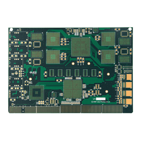
OurPCB fabricates EV charger (electric vehicle charger) PCBs from 2 to 32 layers, including rigid, flex, and rigid-flex stack-ups. Standard builds use FR4 or high-Tg FR4 (up to 180 °C Tg), with support for halogen-free, ceramic-filled, and polyimide substrates where thermal resistance or insulation integrity is required. Hybrid builds combining FR4 and PTFE or ceramic layers can be produced up to 16 layers with engineering review.
We support overall board thicknesses from 0.2 mm to 8.0 mm, with finished copper weights from 1/3 oz to 15 oz. Internal copper distribution is engineered to manage layer-specific current loads in AC or DC power sections, with stack-up validation provided for impedance matching and creepage (surface spacing between conductors to prevent arcing) compliance.e. Dielectric materials include ITEQ IT180A, Isola 370HR, and TUC TU-872 for high-voltage durability and low Dk stability across frequency.
OurPCB supports tight dimensional control and fine-feature fabrication for EV charger PCBs operating at high voltage and high current. Standard trace widths and spacing down to 0.05 mm (2 mil) are achievable with LDI exposure and precision etching, depending on copper weight and layer count. For inner layers, 3/3 mil design rules are supported on 35 µm copper; outer layers can reach 2.5/2.5 mil with 30 µm finished copper.
Minimum mechanical drill diameter is 0.15 mm, with aspect ratios up to 10:1 for plated through holes. Via-in-pad, back drilling, and controlled-depth milling are available for fine pitch designs and high-speed signal routing. Board outline tolerances are held to ±0.1 mm, with hole position accuracy to ±0.075 mm.
Standard thickness tolerance is ±10% for boards ≤1.0 mm and ±7% for boards between 1.8 mm and 4.0 mm. All fabrication steps are governed by IPC-6012 and IPC-2221 design standards for Class 2 and Class 3 performance targets.
Standard finishes include lead-free HASL, OSP, ENIG, immersion silver, immersion tin, and hard gold plating. These options are selected based on end-use application, required contact durability, and environmental exposure.
ENIG (Electroless Nickel Immersion Gold), a corrosion-resistant nickel-gold surface finish, provides excellent planarity and corrosion resistance, making it ideal for connector pads and surface-mounted components in AC and DC charging modules. Immersion silver is available for high-speed signal layers requiring low contact resistance. Hard gold is used for edge connectors or gold fingers subjected to repeated mechanical wear.
All surface finishes are RoHS-compliant and applied in controlled chemical environments with line-level inspection for thickness, solderability, and uniformity. Selective finish combinations, such as ENIG with hard gold edge fingers or OSP over inner copper layers, are supported to meet mixed interface requirements in EV charging systems.
OurPCB provides end-to-end assembly services for EV charger PCBs, supporting both surface mount and through-hole technologies. SMT lines handle fine-pitch components down to 0201 packages, with placement accuracy of ±25 µm and reflow profiles optimized for multilayer high-copper boards. Nitrogen reflow is available for oxidation-sensitive assemblies, especially in high-voltage applications.
We support THT processes for connectors, relays, and large passive components using wave soldering or selective soldering with controlled thermal gradients. Double-sided reflow, mixed technology, and BGA rework services are also available. BGAs are aligned using optical centering and inspected post-process with 5 µm resolution X-ray systems.
All assembly steps follow IPC-A-610 Class 2 or Class 3 criteria, with real-time process monitoring for solder paste volume, placement alignment, and joint integrity. ESD-safe material handling, moisture-sensitive device (MSD) tracking, and batch-level lot control are standard across both facilities.
OurPCB integrates inline inspection and electrical test systems throughout the EV charger PCB assembly process to verify build quality, functional integrity, and regulatory compliance. Automated Optical Inspection (AOI) is used after solder paste printing and post-reflow to detect component skew, tombstoning, insufficient solder, and polarity errors across all SMT placements.
For assemblies with BGAs, QFNs, or embedded pads, real-time X-ray inspection validates solder joint formation and detects voids, bridging, or incomplete wetting. All BGA rework is re-inspected post-process. Solder paste inspection (SPI) verifies volume, height, and area coverage before pick-and-place.
In-circuit testing (ICT) is available for populated PCBs with accessible test points, using custom fixtures to measure continuity, resistance, diode orientation, and component presence. High-voltage testing and functional test rigs can be applied at end-of-line for charger boards operating in 220V or 380V systems. All tests follow IPC-TM-650 and customer-specific protocols for yield control and traceability.
OurPCB offers protective coating and environmental sealing solutions tailored to the outdoor and high-voltage demands of EV charger PCBs. Conformal coating, a protective film that shields against humidity, dust, and ionic contamination, is applied by selective spray, dip, or brushing methods using acrylic, silicone, or polyurethane chemistries. These coatings protect against humidity, condensation, dust, and ionic contamination, with thickness control between 25 µm and 75 µm.
We also provide three-proof treatment—moisture-proof, mold-proof, and salt-spray-proof—based on GB/T 4797.6-1995 standards. This process enhances board survivability in outdoor-rated chargers subject to IP54 or IP65 enclosures. Materials are qualified for adhesion, dielectric strength, and thermal cycling resistance.
All coated boards are UV-inspected for coverage uniformity and undergo post-cure verification before final packaging. Optional masking is available for connectors, test points, or edge fingers to maintain electrical interface integrity during the coating process.
OurPCB manufactures EV charger PCBs designed for AC, DC, and AC/DC integrated systems, supporting charger power levels from 3.3 kW up to 30 kW. We fabricate control and power conversion boards for AC Level 1 and Level 2 chargers, DC fast chargers, and bidirectional onboard modules. Each topology requires specific copper distribution, insulation spacing, and thermal design strategies incorporated at the stack-up and layout levels.
For AC designs, we support isolated control PCBs with precise routing for zero-crossing detection, relay actuation, and grid interface circuitry. DC charger PCBs are built for direct high-current transfer, with wide trace widths, heavy copper layers, and reinforced dielectric spacing to meet safety class clearance requirements.
We also support charger architectures using SiC MOSFETs, GaN FETs, and phase-shifted full bridge (PSFB), LLC, or dual active bridge (DAB) converter topologies. Our production team can adapt layer counts, thermal relief, and pad geometry to support each topology’s electrical and mechanical demands.
We support five primary types of conformal coatings, classified by IPC-CC-830B: acrylic (AR), silicone (SR), epoxy (ER), polyurethane (UR), and parylene (XY). Each coating type offers distinct electrical, thermal, and chemical properties suited to different operating conditions and board requirements.
| Coating Type | Properties | Application Range | Process Characteristics |
|---|---|---|---|
| Acrylic (AR) | Dielectric strength up to 100 kV/mm; moderate moisture resistance; UV resistant. | Consumer electronics, industrial controls, PCBs not exposed to aggressive chemicals. | Fast air-dry or heat cure at 60 to 80 °C; removable with isopropyl solvent; 25 to 75 µm films. |
| Silicone (SR) | Operating range –55 °C to +200 °C; flexible after cure; resists condensation cycling and salt spray. | Automotive PCBs, aerospace systems, outdoor and high-vibration PCB assemblies. | Long open time; cures at room temp or with heat; film builds 50 to 250 µm. |
| Epoxy (ER) | Rigid, high-hardness film; excellent chemical resistance; dielectric withstand up to 1500 V. | Hazardous environments, fuel-exposed zones, sealed sensor PCBs. | 2-part systems with limited pot life; cure at 100 to 150 °C; not reworkable; 50 to 125 µm thick. |
| Polyurethane (UR) | Excellent abrasion, solvent, and hydrocarbon resistance; dielectric insulation ≥80 kV/mm. | Automotive ECUs, power inverters, heavy industrial and under-hood electronics. | UV-curable or heat-cured; flexible or rigid grades; thickness 50 to150 µm. |
| Parylene (XY) | Pinhole-free, uniform film; dielectric strength ~7000 V/mil; barrier to moisture, oxygen, and chemicals. | Aerospace, implantable devices, optics, MEMS, RF components. | Applied via vapor deposition at ambient temp; 10 to 25 µm build; no masking needed. |
We use four primary coating methods selected based on material class, board geometry, and coverage tolerance: selective spray, manual spray, dip coating, and vapor deposition.
This method uses 3- or 4-axis gantry systems with precision atomizing nozzles and programmable XY motion.
Nozzle height, angle, and flow rate are calibrated per coating type, maintaining zone resolution within ±0.5 mm and film thickness uniformity within ±10%.
Ideal for high-density PCB assemblies with exposed test points, edge connectors, or variable component height.
Used for low-volume prototypes, repairs, or geometries unsuitable for automation.
Operators control fan angle, fluid pressure (15 to 30 psi), and standoff distance to apply coatings in layers of 25 to 75 μm.
Applications are validated visually and under UV light to confirm consistent wet-out, no edge pullback, and full coverage.
This method involves vertically immersing the printed circuit board in a controlled-volume reservoir.
Withdrawal speeds are set at 25 to 50 mm/s, depending on coating viscosity and required film build.
Dip angle and flow rate are adjusted to minimize trapped air under low-clearance components.
Film thickness is influenced by surface tension and cure rate, and is commonly used for uniform coverage on conformal-only builds without selective masking.
Parylene is applied using a vacuum-based process that converts solid dimer into a gas-phase monomer, which deposits and polymerizes on all exposed surfaces.
This technique coats the substrate uniformly, including sharp edges, recesses, and vertical sidewalls, with thickness variation held within ±1 μm.
Parylene is used on MEMS, high-voltage analog boards, and RF assemblies requiring stable dielectric properties across small geometries.
Coverage and film integrity are verified through mass gain measurements, microscopic cross-sections, and electrical breakdown testing at defined voltage intervals.
Our PCB conformal coating services are used in high-reliability sectors where exposure to humidity, contaminants, vibration, or voltage stress can degrade unprotected circuitry. Each industry imposes specific insulation resistance, material compatibility, and verification requirements, which we address through material selection, validated cure profiles, and documented inspection.
We coat assemblies for airborne control units, telemetry modules, and radar interfaces using parylene coating and MIL-I-46058C qualified epoxy resin systems.
Coatings are applied to maintain dielectric integrity ≥100 MΩ under IPC-TM-650 Method 2.5.5.1 and to pass thermal shock (-55 °C to +125 °C, 100 cycles) and salt fog per MIL-STD-810.
For mission-critical analog or RF boards, coating thickness is between 12 and 25 μm via calibrated vapor deposition, and selective masking jigs maintain conductor exposure for shielded components.
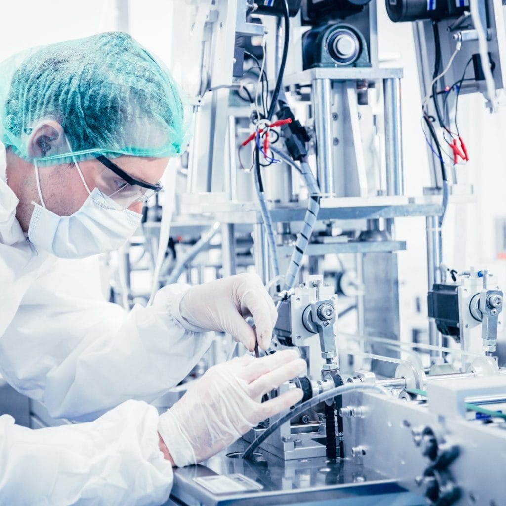
We support ISO 13485 traceability and FDA Class II/III product readiness for coated PCBs in implantable monitors, handheld diagnostics, and drug delivery pumps.
Our materials include low-VOC acrylic conformal coatings, silicone systems with biocompatibility screening (ISO 10993), and low extractables.
Boards are cleaned to <1.56 μg/cm² ionic contamination before coating application, and inspection includes blacklight coverage validation and adhesion per IPC-CC-830B Section 3.4.3.
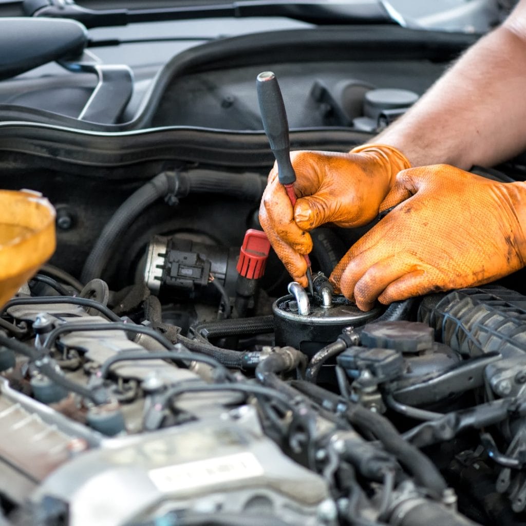
We apply high-flexibility polyurethane coating and thermal-grade silicone resins to BMS, powertrain, and infotainment boards exposed to rapid temperature change (–40 °C to +150 °C), vibration, and condensation cycling.
Conformal coating increases isolation between power planes and prevents dendritic growth from conductive dust or condensation.
We validate the coating process with cross-section analysis (MIL-STD-883 Method 5011), cure retention, and adhesion resistance to brake fluid, fuel vapor, and engine oil splash.
Our coating lines support PLC, inverter, and SCADA system boards exposed to particulates, ozone, and wide humidity swings.
For boards mounted in IP65/67-rated enclosures, we apply hydrophobic conformal coating materials using 3-axis selective spray with edge-lead clearance masks.
Boards operating near high EMI sources are coated with carbon-filled urethane blends that suppress parasitic discharge and pass 1500V dielectric withstand per IPC-TM-650.
Coated assemblies are baked and UV-cured depending on the chemistry used, with full batch lot tracking and AOI confirmation.
Conformal coatings provide electrical isolation, environmental protection, and mechanical stability for PCB assemblies in uncontrolled or high-risk environments. Benefits are measurable across insulation resistance, failure rate reduction, and extended service life under sustained load or contamination exposure.
Conformal coatings increase surface resistance between conductors, raising dielectric withstand voltage and minimizing leakage current. A 50 μm acrylic layer can support insulation resistance above 100 MΩ at 500 VDC. This allows tighter conductor spacing without breakdown, essential for high-density or high-voltage assemblies.
Coatings act as moisture and particulate barriers, preventing water absorption, salt bridging, and chemical penetration. Properly applied coating halts the formation of dendrites and suppresses metal migration, even in humidity cycling from 20% to 95% RH. Boards operating near HVAC units, marine environments, or corrosive gas sources gain long-term stability through controlled coating coverage.
Coated assemblies resist vibration-induced solder fatigue, abrasion during handling, and surface contamination from oils or flux residues. Flexible coatings such as silicone accommodate mechanical deflection and substrate expansion while maintaining adhesion, which is key in applications with wide temperature ranges or cyclic stress.
By sealing exposed conductors and insulating critical components, PCB conformal coating reduces the occurrence of short circuits, corrosion-based failures, and oxidation-driven resistance drift. This increases overall system uptime and reduces warranty or service intervention, particularly in automotive, industrial, and outdoor deployments.
Mon-Fri: 24 hours,
Sat: 9am-6pm, GMT+8
Reach us at
sales@ourpcb.net
24 hours online
+86-199-30589219
Mon-Fri: 24 hours
Sat: 9am-6pm, GMT+8
Conformal coating is a thin polymer film (25 to 250 μm) applied to a printed circuit board to increase surface insulation resistance, suppress ionic conduction, and prevent corrosion under high humidity or airborne contamination. The coating conforms to irregular geometries (pins, vias, SMDs), forming a uniform dielectric barrier with no voids or air gaps.
This process blocks moisture ingress, inhibits dendritic growth between closely spaced traces, and maintains>100 MΩ insulation resistance as measured by IPC-TM-650 Method 2.5.5.1. By controlling coating thickness and zone coverage, we support IPC-CC-830B electrical class builds, including compact high-voltage designs and analog assemblies sensitive to leakage or noise coupling.
We maintain uniformity and coverage in our PCB conformal coating service by controlling every variable in the coating process, from substrate prep to final inspection.
Boards are cleaned to <1.56 μg/cm² ionic contamination (per IPC-TM-650 2.3.25) and pre-baked to remove residual moisture. PCB coating is applied with calibrated equipment: spray nozzles are set for defined atomization angle, flow rate, and pass overlap; dip speeds are held within ±5 mm/s.
Coating thickness is verified at multiple zones using ultrasonic or eddy current gauges, targeting 25 to 100 μm depending on dielectric clearance and material class. Post-cure inspection includes UV light for coverage, black spec detection, and edge masking accuracy.
AOI and fixture-based GO/NO-GO templates are used for selective coating services. All inspection and process parameters are documented per lot with time-stamped operator traceability.
Repair starts with identifying the coating type. Acrylic is removed using isopropyl or butyl acetate solvent, while polyurethane and cured epoxy coatings require micro-sanding or localized thermal scraping. Removal is confined to the defect area, using precision masking and anti-static tools to protect adjacent traces.
After re-exposure, the board is cleaned (<1.56 μg/cm² NaCl equivalent), dried, and re-coated using brush or precision air-dispense. The repair zone is cured per original material spec and verified under UV light for uniform edge blend and full coverage. Adhesion is confirmed with IPC-TM-650 Method 2.4.1, and dielectric isolation is retested where required.
All rework is documented by lot, technician ID, and re-inspection record.
We provide a custom PCB conformal coating service by defining all parameters at the DFM stage. This includes evaluating component standoff height, clearance zones, dielectric targets, and exposure class. Material selection is based on required dielectric strength, cure profile, and compatibility with soldermask, silkscreen, or exposed metals.
For selective coverage, we use fixture-based masking or laser-cut templates to hold edge definition within ±0.5 mm. Cure parameters are matched to each coating material, with thermal ramp and dwell validated for reflowed assemblies. If dual-material systems are needed (e.g. parylene coating over epoxy-sealed areas), we stage deposition under vacuum after pre-seal application.
Final validation includes UV coverage check, adhesion pull (per IPC-TM-650 2.4.1), and insulation resistance retest if high-voltage spacing is affected. All deviations and re-qualification steps are recorded by lot.
OurPCB delivers controlled, standards-aligned PCB conformal coating services with full traceability, inline inspection, and integration with PCB assembly and test. Contact us to discuss your build, define your coating requirements, or request a quote for your next project.
When asked why Apple manufactures in China, ‘cheap labor’ is the facile answer. The more accurate one is supply chain engineering. A modern iPhone may

PCB tariffs from China can significantly change the real cost of a U.S.-bound order before your boards reach production. A quote may look competitive at

Wire harness tariffs from China commonly fall under HTS 8544.30, the U.S. Harmonized Tariff Schedule (HTSUS) classification for ignition and other wiring sets used in

Unverified wire harness suppliers pose significant risks that often surface long after delivery. A weak crimp, wrong insulation material, missing UL rating, or undocumented connector

Placing an initial Purchase Order (PO) with an unverified China-based PCB supplier can critically jeopardize your budget, launch timeline, and product quality. Knowing how to
Underwriters Laboratories (UL) help engineers, buyers, and manufacturers choose wire and cable that can safely perform in specific electrical, mechanical, and environmental settings. These standards
Quick-turn conformal coating for prototypes with multiple material options.
Selective spray or dip coating with IPC-compliant thickness verification.
Cost-optimised high-volume conformal coating with automated inspection.
Re-ordered conformal-coated PCBs twice this year, same solid result.
Careful packaging on the conformal-coated PCBs and complete documentation.
Communication during the conformal-coated PCBs build was responsive even across time zones.
The conformal-coated PCBs came back flawless — tight tolerances and a clean soldermask finish.
Their engineers flagged two DFM issues on our conformal-coated PCBs before production — saved us a respin.
We use cookies to improve your browsing experience, which may include personal information. By clicking "Agree," you accept our Privacy Policy and cookie use. You can change your cookie settings in your browser anytime.
Agree Chat With Us
  Free Quote