
Top 7 Truck Wiring Harness Manufacturers
Truck wiring harnesses are the electrical backbone of commercial vehicles, from long-haul trucks to construction fleets and emergency vehicles. They must withstand continuous vibration, thermal

Are you looking for advanced microelectronic interconnection solutions that maximize performance while minimizing footprint? OurPCB’s flip chip bonding service delivers industry-leading precision, reliability, and technical capability for your most demanding electronic assembly requirements.
Our state-of-the-art flip chip technology enables direct electrical connection of face-down electronics onto substrates through conductive bumps, offering significant advantages over traditional wire bond approaches in performance, size, and reliability.


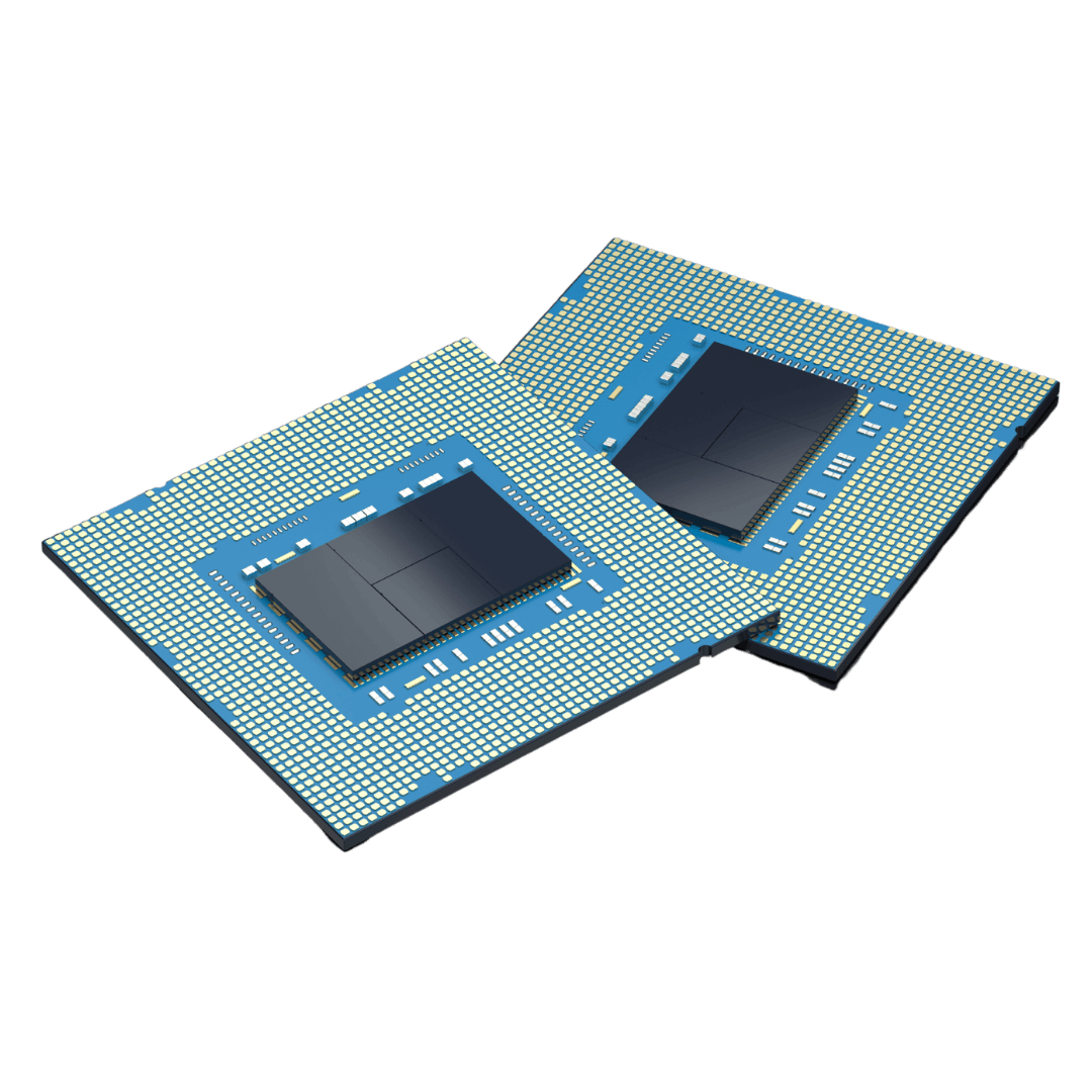

Flip chip technology is a microelectronic assembly method where semiconductor devices are mounted face-down on substrates using conductive bumps. This direct chip attach technique inverts (“flips”) components, so their bond pads face downward to align with matching substrate pads, eliminating the need for wire bonds. The technique creates significantly shorter electrical paths, improving signal integrity while reducing the assembly’s size and profile.
Originally referred to as flip chip or controlled collapse chip connection (C4), this interconnection method has become essential for modern electronics where space constraints, performance requirements, and reliability are critical factors. The flip chip process creates interconnections that outperform traditional wire bonding in terms of electrical performance, thermal management, and miniaturization capabilities.
| Feature | Flip Chip Package | Wire Bond Package |
|---|---|---|
| Connection Type | Direct through conductive bumps | Wire loops from chip edges |
| Size | Compact (chip scale) | Larger (requires perimeter bond area) |
| Signal Performance | Excellent (short connections) | Good (longer wire paths) |
| Thermal Performance | Superior (direct heat transfer) | Moderate (indirect heat path) |
| Manufacturing Complexity | Higher (requires bumping process) | Lower (established process) |


Flip chip packaging delivers superior performance advantages over traditional packaging methods for electronic assemblies requiring miniaturization and enhanced functionality. The technology’s unique structure fundamentally changes how components connect to substrates, enabling benefits that directly impact product performance, reliability, and form factor.

OurPCB stands apart in the flip chip bonding market through our combination of technical expertise, advanced equipment, quality processes, and comprehensive service offerings. We’ve built our reputation on delivering exceptional results for the most demanding applications across industries from telecommunications to medical devices.

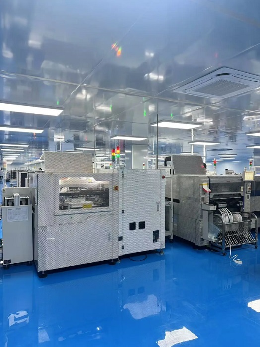
OurPCB delivers a broad selection of PCB assembly services tailored to meet diverse project demands. We prioritize precision, speed, and quality control throughout every phase of the assembly process.
We specialize in Surface Mount Technology (SMT) assembly, ideal for producing compact and high-performance devices. Using cutting-edge pick-and-place machines, we ensure accurate and reliable component placement.
We offer flexible assembly options to fit your project needs. You can supply your own components, or choose our full turnkey service, which includes sourcing, assembly, and final delivery.
Our custom assembly service is designed to accommodate your unique designs and specifications. We handle complex configurations and special requirements, working closely with you to fulfill your exact needs.
We focus on providing fast and dependable PCB assembly. Our quick turn service guarantees high-quality boards delivered within tight deadlines, without sacrificing quality.
We manufacture PCBs that comply with IPC Class 3 standards, essential for critical sectors like aerospace and medical. These assemblies offer the highest reliability for demanding applications.
We assemble all varieties of IC packages with precision, including BGAs, POPs, CGAs, QFNs, DFNs, and CSPs. Our advanced equipment is capable of handling even the most complex IC packaging requirements.
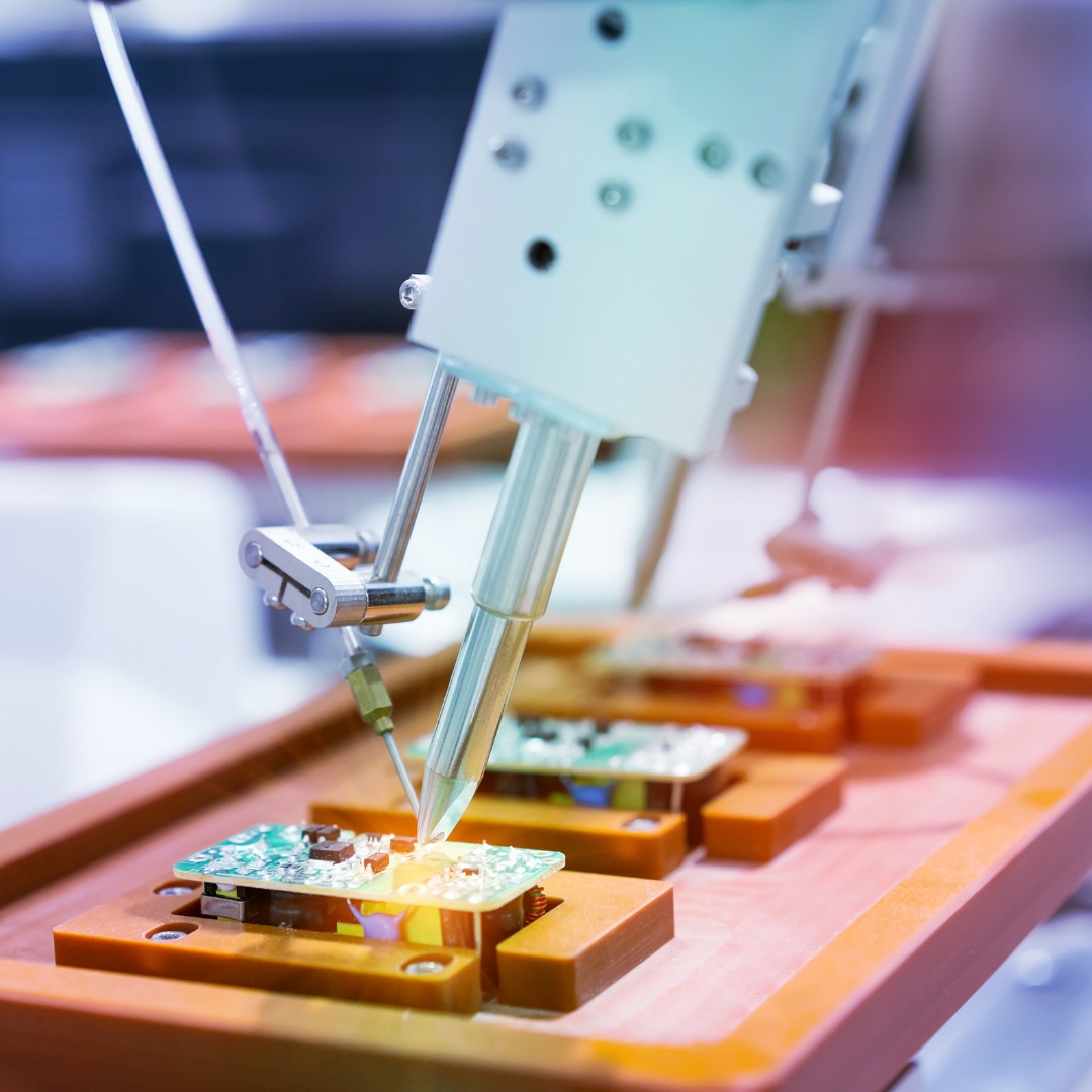
The flip chip assembly process begins with bump preparation on the die pads, creating raised electrically conductive structures that will form connections. OurPCB offers multiple bumping options including solder ball attach (to 305μm diameter), gold stud bumping (pitch down to 150μm), and anisotropic conductive adhesive for specialized applications. After bumping, components undergo precision placement where they’re inverted and aligned to PCB pads with accuracy to 0.5μm using advanced optical systems.
The bonding phase secures the semiconductor devices to substrates through various methods, including thermo-compression (for highest accuracy), thermosonic process (lower temperature), and hot air reflow for various solder types. Finally, the underfill process injects specialized epoxy material in the space between the die and the substrate, which distributes thermal expansion mismatch stresses and protects interconnections from environmental factors. OurPCB offers both standard and reworkable underfill options depending on your specific application requirements.
| Process Step | OurPCB Capability | Technical Benefit |
|---|---|---|
| Solder Ball Bumping | 305μm diameter on 508μm pitch | Optimized for larger die with higher I/O counts |
| Gold Stud Bumping | Pitch down to 150μm | Ideal for fine-pitch, high-density applications |
| Placement Accuracy | Down to 0.5μm | Ensures perfect alignment for maximum reliability |
| Bonding Methods | Thermo-compression, Thermosonic bonding, Hot air reflow | Application-specific optimization |
Under bump metallization is a critical layer deposited on bond pads before the bumping process. OurPCB implements advanced UBM technologies that create robust interfaces between pad materials and bumps. Our UBM technology:
OurPCB provides multiple bumping technologies to optimize interconnect performance for different applications. Solder bump formation creates precise spherical connections using various alloy compositions including low-temperature (96 °C), eutectic (183 °C), and lead-free (217 °C) options. This versatility allows us to match thermal requirements to your specific substrate and component limitations, ensuring reliable connections without thermal damage.
Gold stud bumping creates highly conductive, fine-pitch interconnections ideal for applications requiring the highest electrical performance. Our capability extends to partial wafers and large die with pitch dimensions down to 150μm. For specialized applications, we also offer conductive adhesive flip chip technologies which provide unique advantages in certain optoelectronic and temperature-sensitive applications where traditional reflow process may not be optimal.
Thermal expansion mismatch between die and substrate materials presents a significant reliability challenge in flip chip assembly. OurPCB implements comprehensive solutions to manage coefficient of thermal expansion (CTE) differences effectively. Our underfill materials are specifically engineered to distribute mechanical stresses evenly across the solder joints during thermal cycling.
We use advanced finite element analysis during the design phase to predict stress concentrations and optimize both underfill selection and bump geometry. Our specialized corner bumping techniques provide additional mechanical reinforcement at the highest stress locations. This extends thermal cycling life by up to 40% compared to standard bump distributions.
OurPCB’s flip chip packaging solution delivers exceptional technical capabilities across all critical parameters. Our placement systems achieve alignment accuracy down to 0.5μm, ensuring perfect registration between die and substrate. This precision extends to components with pitches as small as 100μm, supporting the most demanding miniaturization requirements. Our proprietary bonding profile optimization system ensures ideal temperature and pressure parameters for each unique component combination, significantly reducing stress-related failures.
Our comprehensive flip chip capabilities extend beyond basic bonding to include specialized applications such as optical alignment for photonic devices, 3D packaging configurations, and multi-chip modules. We maintain strict process controls for all critical parameters including temperature profiles, pressure application, and alignment verification.
| Technical Parameter | OurPCB Specification | Applications |
|---|---|---|
| Placement Accuracy | 0.5μm | Optoelectronics, MEMS, High-density interconnect |
| Minimum Pitch | 100μm | Advanced processors, RF modules |
| Alloy Options | 96 °C, 183 °C, 217 °C | Temperature-sensitive components, Standard applications, Lead-free requirements |
| Compatible Substrates | Ceramic, Organic PCB, Silicon, Glass, Flex | Diverse applications across industries |
Mon-Fri: 24 hours,
Sat: 9am-6pm, GMT+8
Reach us at
[email protected]
24 hours online
+86-199-30589219
Mon-Fri: 24 hours,
Sat: 9am-6pm, GMT+8
Traditional chip-on-board techniques directly connect components face-down through conductive bumps, rather than using wire bonds or standard surface mount techniques. This approach creates shorter electrical connections (reducing inductance by up to 90%), significantly smaller package sizes, and improved thermal performance through direct heat transfer to the substrate.
Flip chip technology offers maximum value in projects requiring miniaturization, high-frequency performance, or significant thermal management. Specific applications include RF/microwave communications systems, high-speed digital processors, power electronics requiring efficient heat dispersion, optoelectronic modules, MEMS sensors, and medical devices.
To initiate a flip chip assembly process, you should provide detailed technical specifications including die dimensions, pad layout (with pitch requirements), bump material preferences, substrate material and specifications, operational environment conditions, and performance requirements. CAD files showing pad layouts for both die and substrate are essential for proper alignment planning.
Truck wiring harnesses are the electrical backbone of commercial vehicles, from long-haul trucks to construction fleets and emergency vehicles. They must withstand continuous vibration, thermal

Medical cable assemblies sit at the intersection of electrical safety, biocompatibility, and sterilization durability. For regulated medical devices, OEMs must work with manufacturers that understand
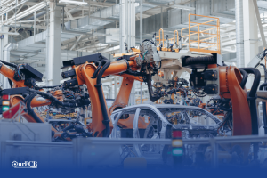
Robotics cable assemblies are unlike ordinary cables, they must survive continuous motion, tight bend radii, torsion, vibration, electrical noise, and often harsh industrial or outdoor
Waterproof cable assemblies have to do more than just “keep water out.” For outdoor, marine, industrial washdown, and transportation platforms, assemblies are expected to survive
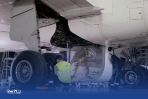
Aerospace cable assembly manufacturers work under standards such as AS9100, ISO 9001, and RTCA/DO-160, and many also maintain ITAR registration to support flight-critical and space-qualified
When considering the best places for manufacturing data cables, China immediately comes to mind. It’s no surprise either — the country has rapidly ascended in
We use cookies to improve your browsing experience, which may include personal information. By clicking "Agree," you accept our Privacy Policy and cookie use. You can change your cookie settings in your browser anytime.
Agree Chat With Us
 Free Quote