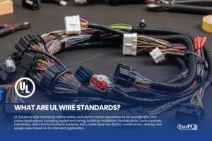
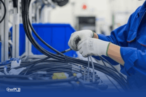
Prototype Cable Assemblies
Prototype cable assemblies are the very important place in between PCB design ideas and interconnects. OurPCB brings prototype assemblies with PCB solutions to your tables.
OurPCB manufactures BT PCBs using certified BT laminate from trusted manufacturers, including Mitsubishi Gas Chemical and Isola.
We fabricate bismaleimide triazine board builds for telecom, computing, and advanced automotive electronics requiring thermal resistance above 356 °F (180 °C).
BT substrates offer low dielectric constant, controlled expansion, and dimensional stability required for high-performance circuit boards used in high-frequency applications.
Each BT resin layer is laminated at 482 °F (250 °C) with a 90-minute dwell cycle using press profiles matched to resin flow rate and glass weave. Layer-to-layer registration is maintained at ±0.0004 inches, with optical alignment verified on every panel.
✅ In-house capability for BT circuit board production up to 40 layers with 0.2 mm to 8 mm thickness.
✅ Minimum 3 mil trace/spacing, 0.075 mm laser drill, and 4 mil annular rings.
✅ All BT resin PCB substrates tested to IPC-6012, ISO 9001, and IATF 16949 standards.
OurPCB manufactures all BT PCBs under ISO 9001, IATF 16949, and IPC-6012 Class 3 certification, with traceability to laminate lot ID, copper foil weight, and surface finish batch. Process control includes XRF-verified plating thickness, AOI image log, and cross-section validation of stackup geometry.
OurPCB operates two ISO-certified manufacturing plants in Shenzhen and Shijiazhuang, each over 10,000 m² and equipped for full-stack BT PCB production. All lamination, drilling, plating, imaging, and testing is executed internally on dedicated process lines.
This eliminates subcontracted subprocesses, cross-contamination risks, and uncontrolled thermal cycles across BT resin builds requiring high glass transition temperatures and dimensional stability.
We build all BT resin PCB material to IPC-6012 Class 2 or Class 3, IPC-A-610, ISO 9001, and IATF 16949 standards. We also hold GB/T42061-2022 for medical electronics and ISO 13485:2016 compliance.
Every job is traceable by laminate lot, surface finish, solder mask ink ID, and copper foil batch. AOI, X-ray, and final inspection are logged per panel per IPC-6012 3.2.1 visual and 3.3.1 dimensional thresholds.
Our team delivers bare BT PCB quotes within 8 working hours, including stackup review, BT resin confirmation, and surface finish selection.
For BT builds with component sourcing or full PCBA, complete quotes are returned within 2 working days. Submissions are reviewed for trace width down to 0.003 inches, copper weight to 3 oz, dielectric spacing, and resin compatibility with press profile requirements.
Materials are sourced from in-stock inventory rated for Tg ≥180 °C and modeled for IPC-6012 Class 3 designs.
We source BT resin PCB material from global suppliers, including Isola, SYTECH, EMC, and Rogers, with each substrate rated for glass transition temperatures from 180 °C to 250 °C (356 °F to 482 °F).
We track every laminate lot ID, copper cladding weight, and resin-glass content for traceable process control.
Material specs are matched to Tg, Dk, filler ratio, and delamination threshold (Td ≥340 °C), ensuring thermal stability across 260 °C reflow and multilayer lamination.
OurPCB uses separate lamination presses, plating baths, oven fixtures, and cleaning chemistries for BT resin builds to avoid FR4 cross-contamination. Drill bits and press tooling are segregated by substrate groups to maintain Tg behavior and resin-glass adhesion consistency.
Lamination presses are profiled for resin flow and dwell control, drill bits are isolated by substrate group, and finish lines are calibrated for adhesion over BT substrate pad geometries.
By isolating fixtures, ovens, stencils, and chemistries from standard FR4 processes, we reduce contamination risk and ensure dimensional repeatability across Class 3 high-density builds.
BT PCBs undergo X-ray, AOI, and ICT testing per panel. Drill diameters (down to 0.003 in), trace width, copper thickness, and via plating depth are logged and inspected against IPC-6012 Class 3-dimensional and visual criteria.
OurPCB delivers full documentation per job: AOI results, plating data, lamination cycle logs, and final cross-section measurements to validate stackup performance, trace uniformity, and structural integrity.
PCB testing services verify electrical continuity, component functionality, and solder joint integrity after the board is assembled. Without complete testing coverage, latent faults such as open circuits, bridged pins, or misprogrammed ICs can escape detection during manufacturing.
Testing ensures that each unit meets IPC-A-610 Class II or Class III workmanship criteria. By combining functional testing, in-circuit testing, and visual inspection, manufacturers can reduce field failure rates, support DFM improvement loops, and maintain traceable quality benchmarks.
Our dual 10,000 m² PCB assembly houses in Shenzhen and Shijiazhuang are equipped with high-speed SMT assembly lines capable of placing fine-pitch parts with ±25 µm tolerance.
Each line includes temperature- and humidity-controlled environments, active anti-static systems, and vacuum transport for handling thin or flex printed circuits.
We are fully certified to ISO 9001, IATF 16949, and IPC-A-610 Class 2 & 3, supporting applications where fine-pitch PCB assembly must meet elevated acceptance criteria for solder joint geometry, lead coplanarity, and component body clearance.
Our QA workflows are built to handle fine-pitch PCBs requiring zero solder bridging and uniform joint fillets across dense arrays.
All assemblies involving ball pitch under 0.5 mm, QFN, or PoP packages undergo X-ray inspection, SPI, and AOI with 15 µm resolution optics.
We detect voids, open leads, insufficient solder, lifted terminations, and hidden shorts. This inspection process is a requirement for successful assembly when working with components that provide no visible solder access.
Every fine-pitch electronic assembly receives a DFM and DFA review focused on stencil coverage, aperture tuning, pcb design limitations, and routing near fine-pitch ICs.
We assist in verifying pad design, thermal pad exposure, and via escape planning, important for high I/O packages like BGA and chip scale layouts where misalignment or solder blockage can compromise yield.
We offer full assembly component sourcing through partners like Digi-Key, Mouser, and WPG, including traceable lots for hard-to-find or moisture-sensitive electronic components.
Components are stored under MSL-compliant conditions, with drying cabinets and vacuum packaging for all incoming fine-pitch parts.
We use vapor degreasing to clean fine-pitch SMT assemblies where low standoff heights prevent rinsing under components. The process heats a fluorinated cleaning fluid such as HFE-72DA until it vaporizes at 58 °C.
Our sealed-chamber systems recover 90% of solvent through closed-loop distillation and vapor filtration. Because no water is used, this PCBA cleaning method prevents capillary trapping and delivers dry, spot-free boards that are immediately ready for conformal coating or inspection.
For high-throughput cleaning, we operate fully enclosed aqueous cleaning systems that combine high-pressure spray with saponified deionized water at 60 °C. These systems target assemblies with solder paste, rosin, or water-soluble flux, removing active ions and organic residue from both sides of the board.
Our InJet platforms use 2.0 bar rotary spray heads for impingement and cascade rinsing with resistivity sensors that maintain <1.56 µg/cm² NaCl equivalent. Each cleaned board is force-dried at 70 °C for 10 minutes to eliminate moisture and prepare the surface for optical inspection or downstream processing. This is the most efficient method for batch-based PCBA cleaning at scale.
When boards require post-assembly rework or selective soldering, we apply a controlled manual cleaning process to treat localized contamination. Technicians begin by applying Decotron T383 or high-purity IPA to the assembly surface, then scrubbing with anti-static brushes at a 45° angle and 250 g pressure.
Flux is then removed using a directional aerosol rinse, and drying is completed with 30 psi filtered air or lint-free polyester wipes. This method allows us to clean the PCBA without subjecting sensitive components to immersion or thermal stress. We document all manual cleaning steps for traceability on high-reliability builds in automotive, medical, and aerospace programs.
OurPCB combines in-house fixture development, multi-platform inspection systems, and Class III process conformance to deliver accurate and reliable results across industrial, medical, and automotive sectors. Each PCB assembly testing service is backed by traceable data, audit-ready reporting, and IPC-certified personnel.
OurPCB integrates PCB testing services directly into SMT, THT, and mixed-technology production lines.
AOI, ICT, and functional test platforms are embedded at key points across our two 10,000 m² facilities in Shenzhen and Shijiazhuang.
Boards pass through automated inspection and electrical test stages without manual handling, reducing contamination risk and improving test repeatability across Class II and III assemblies.
We build all ICT and functional test fixtures internally using CAD-based modeling, high-precision CNC drilling, and pogo-pin calibration systems.
Fixtures are validated for flatness, probe pressure uniformity, and node-to-net correlation before use.
This internal control allows us to shorten test development cycles for new PCB assembly testing services and maintain consistency across repeat orders or multi-site deployments.
Our test infrastructure includes high-speed AOI (25 µm resolution), 5 µm X-ray inspection, 4-wire flying probe testers, and digital high-voltage dielectric testers.
Resistance measurements down to 10 mΩ, voltage capture from 100 mV to 1500 VDC, and insulation resistance over 1000 MΩ ensure detailed diagnostics for every PCB testing service.
Measurement integrity is maintained through ISO-calibrated instruments and logged reference values.
We provide serialized test data with barcode traceability, linking each board to its BOM revision, test station ID, operator, and timestamp.
Reports include fail point coordinates, signal path diagnostics, image references (for AOI/AXI), and environmental test logs.
Our infrastructure supports full compliance with ISO 9001, IATF 16949, and medical-sector audit requirements, making our PCB functional testing services suitable for regulated deployments.
Our testing flows conform to IPC-A-610H Class III for high-reliability electronics, including burn-in testing, dielectric breakdown validation, and full visual and optical inspection of PCBs before final sign-off.
We support test plans that include ESS, startup sequence monitoring, and functional loop stress testing to simulate real-world deployment.
All solder joints, including BGA and QFN, are inspected using 3D AOI and void-mapped X-ray analysis.
Comprehensive quotes for PCB testing services and fixture-based setups are delivered within 48 working hours.
For new PCBA designs, we provide a DFT assessment, pin map verification, and component access review before test planning begins.
This early-stage input improves test coverage, minimizes false failures, and enables rapid onboarding for customers requiring PCB assembly testing services with complex or high-mix builds.
We remove no-clean flux residue because its remaining solids form hygroscopic films with ionic content capable of enabling leakage currents under bias. These residues often contain halide activators or rosin derivatives that, in humid environments, allow ionic mobility as low as 10⁸ Ω insulation resistance across narrow conductor spacing.
On high-density printed circuit board assemblies, especially those with ≤0.3 mm pitch, this can lead to dendritic growth, moisture-induced tracking, and eventual open or short failures. In Class 3 applications, even visually benign residues violate IPC J-STD-001 Section 8.3.1, prohibiting any visible residue under conformal coating.
Removing these residues is required to maintain dielectric performance and prevent latent field degradation.
Our cleaning strategy depends on the flux chemistry and board design. For fully assembled SMT boards, we use vapor degreasing with HFE-72DA or Vertrel XF, which condense at 55 °C – 65 °C onto the PCBA surface, dissolve polar and non-polar residues, and evaporate without leaving water or exposing components to immersion.
In rework areas or where selective cleaning is required, we use Decotron T383 or high-purity IPA with aerosol precision nozzles to rinse solder ball traps and low-solids residue from around pads.
The process is followed by 30 psi filtered air drying or vacuum-assisted drying to prevent water adsorption beneath packages. Surface prep is validated using surface insulation resistance (SIR) measurements, ionic testing (<1.56 µg/cm² NaCl equivalent), and UV light to detect fluorescence from missed residues.
Removing flux residue allows for consistent conformal coating flow and edge adhesion, especially in boards using urethane or acrylic coatings. Cleaned surfaces increase surface energy, improving film wetting and eliminating common defects like dewetting, bridging, or edge lift.
Coating adhesion strength improves from 1.2 N/mm (on flux-contaminated surfaces) to over 2.5 N/mm on properly cleaned copper and solder mask regions, reducing delamination risk during thermal cycling. In addition, a clean PCB surface ensures that automated optical inspection (AOI), UV inspection, or manual visual checks can accurately detect voids, bubbles, or skipped areas.
For applications in automotive ECUs, implantable medical devices, or high-speed digital RF systems, surface cleanliness before coating directly correlates to long-term device reliability in harsh conditions.
BT resin PCB material offers superior thermal stability, dielectric performance, and dimensional control compared to standard FR4. While FR4 is commonly used for general-purpose printed circuit boards, BT substrate systems are selected for high-frequency, high-reliability applications where Tg, CTE, and Dk must be tightly controlled.
Property | BT Resin | FR4 |
---|---|---|
Dielectric Constant (Dk) | 3.2 to 3.5 @ 1 GHz | 4.2 to 4.7 @ 1 GHz |
Dissipation Factor (Df) | < 0.015 | 0.02 to 0.035 |
Glass Transition Temperature | 180 °C to 250 °C (356 °F to 482 °F) | 130 °C to 170 °C (266 °F to 338 °F) |
Z-Axis CTE | < 60 ppm/°C | 70 to 120 ppm/°C |
Moisture Absorption | < 0.2% | 0.3 to 0.5% |
Thermal Decomposition (Td) | ≥ 340 °C (644 °F) | 280 °C to 310 °C (536 °F to 590 °F) |
Drillability | Laser and mechanical to 0.003 in | Typically, 0.008 in and above |
Applications | High-speed, RF, memory, telecom | Consumer electronics, general purpose |
Cost | Higher (2 to 3x panel cost) | Lower |
Lower dielectric constant (Dk) and dissipation factor (Df) values in BT resin reduce signal delay and minimize attenuation in high-speed traces, making it better suited for controlled-impedance and RF designs than FR4.
Higher Tg and thermal decomposition thresholds (Td) allow BT substrates to survive 260 °C reflow cycles without delamination, warping, or resin-glass separation. These advantages make BT resin the preferred PCB material for memory modules, telecom hardware, and advanced computing interfaces.
OurPCB manufactures high-reliability BT PCBs using a step-by-step in-house process that includes material selection, stackup modeling, lamination at 482 °F, laser and mechanical drilling, electroplating, and LDI-based trace imaging.
Each build is constructed from certified BT resin PCB material, processed with fixed press profiles and drill-to-copper targeting for consistent dimensional and thermal performance. Boards are finalized through surface finishing, AOI inspection, and impedance testing to ensure each production stage meets IPC-6012 Class 3 requirements.
OurPCB manufactures BT PCBs with layer counts from 2 to 40, using high-temperature BT resin cores and prepregs rated for 482 °F (250 °C) lamination. All laminate materials are press-profiled using resin content data, Z-axis expansion rate, and dielectric breakdown testing.
Stackups are configured with resin-glass compatibility and modeled for uniform flow and delamination resistance. We verify bond integrity using microsection analysis and cross-layer resin coverage checks in accordance with IPC-6012 Class 3 requirements.
Laser and mechanical systems drill BT resin PCB substrates with microvia diameters down to 0.003 inches and mechanical holes down to 0.006 inches. OurPCB maintains aspect ratios up to 10:1 with ±0.002 inch via-to-target concentricity using X-ray drill alignment.
Resin smear removal, desmear chemistry compatibility, and drill depth are matched to the BT substrate type and layer configuration. Every via structure is verified with hole-wall plating measurement and thermal stress testing.
We image BT PCB circuit boards with trace/space down to 0.003 in. / 0.003 in. on 0.5 oz base copper using LDI exposure. Outer-layer image registration is held to ±0.0005 inches, with layer-to-layer alignment verified optically.
Our imaging process supports impedance-controlled structures, matched trace delay, and complex ground/power pair routing. Finished trace geometry is validated with cross-section inspection and etch factor compensation for high-performance RF and memory designs.
OurPCB plates inner layers up to 2 oz and outer layers up to 3 oz, maintaining ±10 percent plating uniformity across all surfaces and hole walls. We process BT resin PCB material using plating chemistries optimized for surface adhesion and low void rate.
Finished copper thickness is measured on both surface traces and via walls using inline XRF scanners, held to ±10% uniformity per IPC-6012 Class 3 standards, and confirmed post-etch by calibrated micrometer on etched coupons. This ensures thermal performance and current carrying capacity are matched to the BT PCB layout and stackup.
We process bismaleimide triazine and BT-epoxy hybrid resin systems rated for sustained exposure to 500 °F lamination and multiple thermal excursions. Our material systems meet Tg ≥180 °C and Td ≥340 °C, verified by TMA and DSC analysis.
Boards are modeled for resin-glass interface control and undergo T288 delamination testing to confirm reflow stability. These materials are used in high-performance electronic devices, RF modules, and multilayer PCB applications requiring dimensional reliability and thermal endurance.
We manufacture BT PCBs up to 20 × 47 inches, with board thickness from 0.008 to 0.315 inches, controlled to ±10 percent on finished builds above 0.039 inches. Thickness validation is performed using automated height probes and cross-sectioned panel samples.
Edge-to-edge dimensional tolerance is held within 0.004 inches using optical routing and V-cut tooling. These tolerances ensure fit and planarity in connectorized, embedded, and rigid-flex assemblies using BT resin PCB material.
OurPCB manufactures BT PCBs for high-reliability systems in telecommunications, automotive control, aerospace platforms, and medical instrumentation. These industries demand dimensional stability, low dielectric constant, and consistent plating under thermal and mechanical stress.
BT PCBs are used in baseband units, transceiver modules, and phased-array RF components operating at frequencies above 6 GHz.
Boards are built with matched-impedance traces, low-Dk materials, and plated vias capable of maintaining signal integrity through multi-cycle reflow and high temperatures in the field.
BT substrate boards are used in airborne radar, control avionics, and mission-specific processing systems.
We manufacture these circuits using stackups rated for 482 °F lamination, copper plating to 2 oz, and dimensional tolerances below 0.004 inches across 16 to 30-layer builds.
Our BT PCBs are used in ultrasound systems, patient monitoring circuits, and digital imaging control boards.
Resin systems are selected for low moisture absorption and dielectric stability, with trace width control down to 0.003 inches and validated solder joint reliability across multiple sterilization cycles.
BT resin stackups are used in memory modules, SSD controllers, and FPGA interface boards requiring low dissipation factor and trace skew management.
Signal layer matching and plated via consistency are controlled for timing-critical interfaces at DDR4 and PCIe Gen4 speeds.
Mon-Fri: 24 hours,
Sat: 9am-6pm, GMT+8
Reach us at
[email protected]
24 hours online
+86-199-30589219
Mon-Fri: 24 hours,
Sat: 9am-6pm, GMT+8
BT stands for bismaleimide triazine, a thermoset resin used as the base of the BT resin PCB material stackup. It’s formed by polymerizing bismaleimide and triazine monomers into a cross-linked structure with high thermal and electrical stability.
As a substrate material, it offers a glass transition temperature (Tg) between 180 °C and 250 °C (356 °F to 482 °F) and a dielectric constant (Dk) between 3.2 and 3.5 at 1 GHz, making it suitable for multilayer BT PCBs in high-frequency digital and RF applications.
BT resin is a thermoset polymer synthesized by reacting bismaleimide (BMI) with cyanate esters, which cure into triazine ring structures during thermal processing. This cross-linked network creates a high-strength molecular backbone that delivers glass transition temperatures (Tg) between 180 °C and 250 °C (356 °F to 482 °F) and Z-axis expansion rates below 60 ppm/°C.
The bismaleimide component enhances mechanical rigidity and thermal resistance, while the triazine groups reduce dielectric loss and moisture absorption. BT resin is often modified with epoxy resin or inorganic fillers to adjust flow behavior, CTE alignment, and prepreg bond uniformity across multilayer stackups. These properties enable bt resin pcb material to maintain structural and electrical performance during multilayer lamination, reflow, and high-frequency signal propagation.
BT resin was developed in the 1970s by Mitsubishi Gas Chemical Company (MGC) to meet the aerospace sector’s demand for thermally stable, high-Tg packaging substrates. The material is synthesized from bismaleimide and triazine compounds, forming a thermoset polymer with excellent dielectric strength and thermal endurance.
In 1985, BT resin was adopted by the semiconductor industry as a cost-effective alternative to ceramic substrates for chip packaging. Its ability to maintain structural integrity during wire bonding, reflow, and molding cycles made it ideal for CSPs and memory modules. Today, MGC supplies over 90% of the global BT resin market, positioning BT as the industry standard for high-reliability, high-density interconnect builds.
BT resin PCB material enhances thermal management through its high thermal decomposition temperature (Td ≥340 °C), low CTE, and high glass content. The resin-glass interface prevents delamination during thermal shock, while its structure allows consistent via plating and surface planarity under multi-reflow conditions.
BT laminates in power modules and control systems enable heat dissipation across copper planes and minimize thermal gradient deformation. Testing includes T288 delamination cycles, Td via DSC, and interlaminar peel strength.
Yes, BT substrate material maintains low moisture absorption rates below 0.2% by weight, making it suitable for applications exposed to reflow, cleaning, or high-humidity environments. Its tightly cross-linked polymer network resists hydrolysis and ion migration, preventing dielectric degradation and delamination.
OurPCB verifies moisture sensitivity level (MSL) performance using pre-bake cycles, outgassing analysis, and reflow simulation per J-STD-020 and J-STD-033 standards for BT resin PCB storage and handling.
BT PCBs fabricated from bismaleimide triazine exhibit flexural strength above 50,000 psi, high hardness, and excellent dimensional stability. They resist warpage and via fracture under mechanical stress due to their low Z-axis expansion and uniform glass reinforcement.
Drilling quality is enhanced by the material’s hardness and brittleness balance, enabling clean microvia formation. Mechanical strength is validated using IPC-TM-650 test methods for peel strength, flexural modulus, and thermal stress performance.
Request a quote and get stackup modeling, material confirmation, and support from a certified manufacturing team. We’ll review your design for layer count, finish compatibility, and thermal requirements, and return a detailed quote within 2 business days.
Prototype cable assemblies are the very important place in between PCB design ideas and interconnects. OurPCB brings prototype assemblies with PCB solutions to your tables.
PCB thermal management prevents component overheating through strategic heat transfer techniques. Without proper thermal control, electronics are at risk of electronic failures through weakened solder
ContentsKey TakeawaysWhat is a Multilayer-Printed Circuit Board?How do Multilayer PCB Boards Work?Multilayer PCB ApplicationsMultilayer PCB Manufacturing Process: StepsMultilayer PCB Manufacturing MachinesBenefits of Multilayer Circuit BoardsWhat
As electronics continue to miniaturize while processing power increases, the resulting thermal challenges make high-Tg PCBs increasingly essential for modern electronic design. ContentsKey TakeawaysWhat is
Running a computer system requires computer memory. In the entire computer system, it’s one of the vital components. Therefore, it’s important that you have basic
Electronic enthusiasts developing a circuit project may want to think about whether or not they should integrate an FFC vs. FPC. Both cables possess varying
We use cookies to improve your browsing experience, which may include personal information. By clicking "Agree," you accept our Privacy Policy and cookie use. You can change your cookie settings in your browser anytime.
Agree