
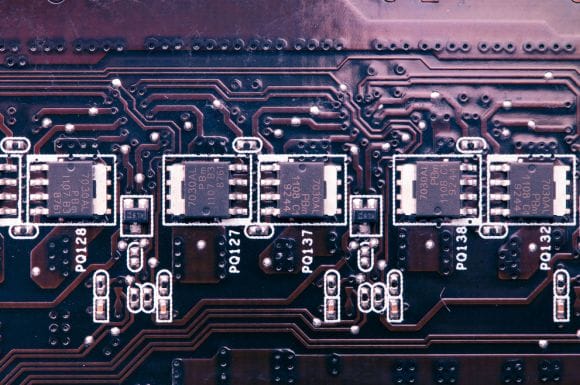
Impedance Control PCB Prototyping & Manufacturing
OurPCB provides PCB manufacturing and prototyping services with a focus on controlled impedance to support high-speed signal performance. Controlled impedance ensures signal integrity in high-speed PCB designs by maintaining consistent impedance throughout traces. We design printed circuit boards with impedance requirements tailored for reliable performance in RF, high-speed digital, and mixed-signal applications.


What is Impedance Control in PCB?
As electronic devices advance, they use more powerful components and drivers that communicate through high-power, high-frequency signals. Traditional copper signal trace designs are not capable of handling this performance. However, you can design a controlled impedance PCB to take care of this.
With PCB-controlled impedance, you get several improvements, such as thicker and wider copper traces to transmit high-speed signals. At OurPCB, our manufacturing process places a focus on controlled impedance designs to ensure optimal performance for high-speed applications. If you’re interested in our services, feel free to request a PCB assembly quote to learn more!
PCB Manufacturing Process


What is Impedance?
Impedance is a measure of the total opposition that a circuit presents to alternating current (AC) when a voltage is applied. An impedance value is usually represented by the symbol Z and is measured in ohms (Ω). Moreover, impedance is an important concept in electrical engineering and electronics.
Specific impedance values can vary depending on the application and the specific requirements of a circuit. Here are a few common impedance values used in electronics and PCB impedance design:


Standard impedance value used in many high-frequency applications, including radio frequency (RF) circuits and test equipment
Used in video and cable television applications
Often used in differential impedance signaling applications, such as Ethernet and USB
Used in some antenna systems and older television applications
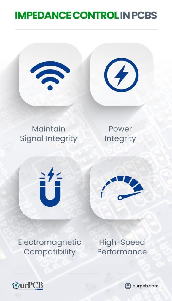
Why is Impedance Control Important in PCBs?
Let’s get into why PCB impedance control is important. Essentially, it plays a major role in high-speed and high-frequency PCB designs. It improves the performance and reliability of electronic devices. Here are a few other reasons why impedance control is influential in PCBs.
Maintain Signal Integrity
With controlled signal integrity, you will have clean and reliable PCB signal traces and transmissions. A controlled impedance trace can minimize signal reflections and distortions and can maintain quality over a long PCB trace.
With a trace impedance mismatch, you may be faced with increased rise and fall times, ringing and overshoot, false logic circuit triggers, and more.
Power Integrity
Impedance control can help manage power distribution and reduce noise in power delivery systems. Essentially, maximum power is transferred only when the source impedance matches the load impedance.
In PCB assembly and design, a controlled PCB transmission line will ensure efficient power delivery to components and optimize signal strength in communication systems.
Electromagnetic Compatibility (EMC)
When you specify impedance control in PCBs, you can minimize electromagnetic interference (EMI) and improve the overall performance of your system. Impedance control is also important for meeting regulatory requirements, reducing interference with other devices, and improving overall system reliability, all of which contribute to maintaining optimal signal integrity.
High-Speed Performance
A PCB manufacturer will ensure impedance control because it’s essential for high-speed digital circuits. It is also incredibly important for RF and microwave applications.
How to Achieve Impedance Controlled PCBs
Achieving uniform controlled impedance in a PCB involves careful planning, design, and manufacturing considerations. Here’s a step-by-step guide to help you understand how to achieve controlled impedance at each point.
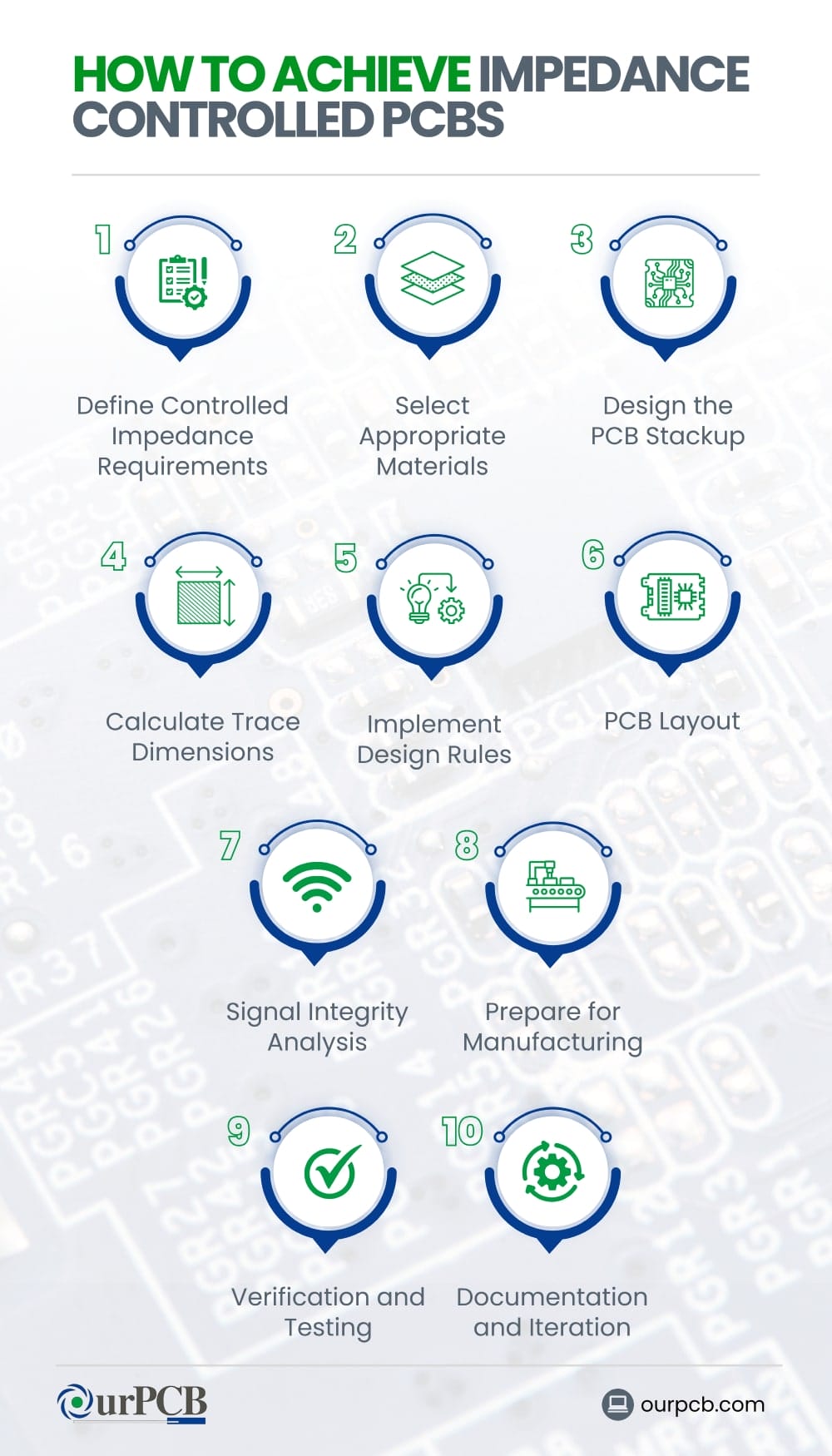
1. Define Controlled Impedance Requirements
The first step is to define your impedance target. For single-ended traces on the PCB, the most common values are 50 Ω, 75 Ω, and 100 Ω. Differential pairs are 90 Ω, 100 Ω, and 120 Ω. Then, you’re going to have to determine the frequency range of operation, as this affects the material selection and design rules.
Finally, specify your impedance tolerance limits. This is usually about 10%, but it can be tighter for more critical applications.
2. Select Appropriate Materials
It’s important to choose the right PCB stackup. Select FR-4 for lower frequencies, but select high-frequency laminates for RF applications.
Lower dielectric constant (Dk) materials typically offer improved performance, while lower dissipation factor (Df) reduces signal loss. Then, be sure to choose the correct copper weight, often between 0.5 to 2 oz per square foot
3. Design the PCB Stackup
Start by figuring out how many layers you’ll need; more layers provide you with better control, but they also increase the cost.
Arrange the signal and plane layers, typically as signal-ground-power-signal. Then, you’ll calculate the dielectric thickness using impedance calculators or specialized software. For more complex designs, you might want to use buried and blind vias.
4. Calculate Trace Dimensions
Use impedance calculation formulas or software to calculate trace dimensions. You’ll need to determine trace width and spacing and adjust these to calculate the impedance value. Also, keep in mind manufacturing tolerances. If you have differential pairs, you’ll have to calculate the individual trace width and the spacing between traces.
5. Implement Design Rules
Set up the trace width and spacing rules in your CAD software and define size, spacing, and type via routes. Then you need to establish clearance rules for between traces, pads, and planes. Create length-matching rules for differential pairs.
6. PCB Layout
Place components to minimize critical trace lengths. Route critical signals first with consistent width and smooth bends. Use reference planes for return paths and route differential pairs as parallel, equal-length traces with length matching. Finally, add guard traces and stitching vias to control crosstalk.
7. Signal Integrity Analysis
Start by performing a pre-layout simulation using tools like HyperLynx or HFSS. Then, conduct a post-layout simulation to verify impedance control and make sure to check for reflections, crosstalk, and EMI issues.
Analyze eye diagrams to ensure that signal quality meets specifications and iterate design if necessary by adjusting trace widths, spacings, or stackup.
8. Prepare for Manufacturing
Generate accurate Gerber files and include impedance requirements in fabrication notes. Specify impedance control requirements, including target impedances for different trace types and acceptable tolerance ranges.
Then, request impedance coupons and test structures for impedance verification. Finally, choose a PCB manufacturer experienced in characteristic impedance control, like OurPCB.
9. Verification and Testing
Perform Time Domain Reflectometry (TDR) measurements to verify actual trace impedance. Use Vector Network Analyzer (VNA) for high-frequency testing to measure S-parameters. Then, conduct functional testing to ensure the PCB meets performance requirements. Analyze test results and make adjustments if necessary.
10. Documentation and Iteration
- Document all design decisions and test results
- Create a report detailing impedance control achievements
- Use insights gained to improve future designs
- Consider creating design guidelines for your organization
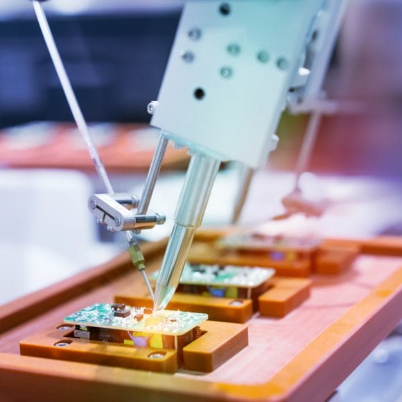
PCB AssemblyServices
We handle everything from parts sourcing to final assembly, providing a hassle-free experience that ensures top-quality boards every time.
Whether you need a few prototypes or large-volume batches, our flexible assembly services adapt to your project’s scope and timeline.
Stay environmentally responsible with our compliant assembly processes, offering RoHS and lead-free options for safe, reliable builds.
No matter the complexity, we can assemble boards of all configurations—single-layer, multi-layer, or a mix—to match your exact specifications.
From one-off prototypes to bulk orders, we accommodate projects of all sizes without compromising on quality or turnaround time.
Join our growing community of satisfied clients who rely on our dependable assembly expertise and dedicated customer support.
Millions of business andinnovatorsuse OurPCB
PCB Board Process
Order Received
- Component Procurement
- Preparation
- PCB Manufacture
- Make Process Flow
Soldering
- Solder Printing/Wave Soldering
- SMT/Plugging
- Inspection (repair if necessary)
- AOI (repair if necessary)
- Transfer
Parts Assembly
- Manual Assembly
- Cleaning
- Wire Screw
- Inspection
- Repair If Necessary
Finalization
- Final Confirmation
- Packing
- Shiping
Technical Capabilities
Capabilities & Services
- One-stop PCBA Services (PCB Manufacturing + Components Sourcing + Assembly)
- SMT Assembly + THT Assembly, Single/double-sided Assembly Mixed PCB Assembly
- BGA Rework
- 60,000 Chips/Hour
- Down to 01005/0210 Size
- Accuracy<±40μm
- Min. QFN Pin Width/Space: 0.15mm/0.25mm
- Min. BGA Diameter/Space: 0.2mm/0.35mm
- Rigid, Flex, HDI, & High-speed Power Boards
- Up to 64 Layers
- 60GHz High Frequencies
- Min. Trace Width/Spacing: 1.8mil/1.8mil
- AOI, X-ray, ICT & FCT Testing
- Controlled Impedance
- ISO 9001, ISO 13485, ISO 14001, IATF 16949, IPC-A-610, UL Certified
- Automotive, Medical, & Military-grade PCBA Manufacturing
Mon-Fri: 24 hours,
Sat: 9am-6pm, GMT+8
Reach us at
[email protected]
24 hours online
+86-199-30589219
Mon-Fri: 24 hours,
Sat: 9am-6pm, GMT+8
FAQ's
What happens if I don't use controlled impedance in my high-speed PCB design?
Without controlled impedance, you can experience unreliable operation, increased bit error rates, and in some cases, complete system failure. Particularly, you might see signal reflections, reduced signal integrity, EMI problems, power loss, and reduced maximum operating frequency.
How does the dielectric constant of PCB materials affect impedance control?
The dielectric constant affects the speed at which signals travel through the PCB. A lower Dk results in faster signal propagation and wider traces. The dielectric constant is an important part of calculating the impedance of a transmission line.
What applications require controlled impedance in PCB designs?
Controlled impedance is essential for ensuring signal integrity in a variety of PCB applications, including:
- High-speed digital systems: Computer motherboards, servers, and networking switches
- RF & microwave equipment: Wireless communications, radar, aerospace, and aviation electronics
- High-speed serial interfaces: USB, HDMI, PCIe, and other data-link standards
- Automotive electronics: ADAS modules, in-vehicle networking, and GPS navigation
- Industrial & telecom gear: Optical network devices, 5G infrastructure, and base stations
- IoT & consumer devices: Smart home hubs, wearables, smartphones, tablets, and HD video equipment
Controlled impedance is also critical in telecommunications and high-speed computing to prevent signal distortion, reflections, and crosstalk.

