
Who are the Top 6 Data Cable Manufacturers in China?
When considering the best places for manufacturing data cables, China immediately comes to mind. It’s no surprise either — the country has rapidly ascended in

OurPCB delivers complete mid volume PCB assembly services tailored to support production volumes of 100 to 5,000 units, bridging the gap between early-stage development and full mass production. By integrating SMT assembly, through-hole assembly, BGA assembly, and in-depth inspection processes, we ensure every product maintains industry-certified reliability standards throughout the assembly process.


Mid-volume PCB assembly refers to production volumes ranging from 100 to 5,000 units, a bridge between prototype validation and full-scale manufacturing. This stage demands careful balancing between flexibility, cost control, and high process consistency to prevent defects from scaling into large production losses.
Mid-volume assembly projects require strict BOM accuracy, stable SMT placement, controlled reflow profiles, and inline defect detection using SPI, AOI, and X-ray systems. Addressing manufacturing challenges early, such as solder voids under BGA packages or stencil alignment issues, ensures first-pass yield rates above 98%, minimizing costly rework at later stages.


OurPCB delivers fully integrated mid volume PCB assembly services, combining PCB fabrication, BOM sourcing, high-precision SMT assembly, selective through-hole soldering, in-line inspection, and post-assembly functional testing under one certified manufacturing system.
Every production run operates under ISO 9001:2015 and IATF 16949:2016 frameworks, with full material traceability and SPC (Statistical Process Control) methodologies applied across each assembly line.
With two factories spanning over 15,000 square meters in Shijiazhuang and Shenzhen, OurPCB supports a wide range of PCB types, including rigid, flex, and rigid-flex printed circuit boards, while maintaining placement accuracy within ±40μm and offering real-time AOI and x-ray analysis on all assemblies.
| Specification | PCBA Capability |
|---|---|
| Placer speed | 600,000 chips/hour |
| Lead Time | 25+ Days (To Be confirmed) |
| SMT | SMT, Through Hole Assembly Single/Double-Side SMT, Single/Double-Sides Mixture Assembly |
| PCB Size | 50mm×50mm ~610mm×508mm |
| PCB Thickness | 0.5mm~4.5mm |
| Min. diameter /space of BGA | 0.2mm/0.35mm |
| Qualifications | ISO 9001:2015 |
| Accuracy | <±30µm, under the condition of 3σ,CPK≥1 |
| Minimum width/space of QFP | 0.15mm/0.25mm |
| Minimum Diameter /Space of BGA | 0.2mm/0.35mm |
| Reliability Test | Flying Probe Test/Fixture test, Impedance Test, Solderability Test, Thermal Shock Test, Hole Resistance Test, and Micor Metallographic Section Analysis, etc. |

OurPCB operates fully automated SMT assembly lines capable of placement accuracy within ±40μm, using high-speed pick and place machines, precision solder paste printers, and SPI systems that inspect paste volume, height, and alignment.
Supported by nitrogen reflow ovens and inline AOI verification, this capability ensures reliable mounting even for 0.2 mm pitch BGAs and 0201-sized passive components, necessary for sectors like medical instrumentation where miniaturization and reliability are non-negotiable.
Dedicated through-hole assembly stations integrate automated insertion and selective soldering processes with manual quality reinforcement for mechanically sensitive components.
Our selective soldering systems apply controlled molten solder precisely at thermal profiles optimized for connectors and high-current components, often used in automotive sensor PCB assemblies requiring rugged mechanical stability.
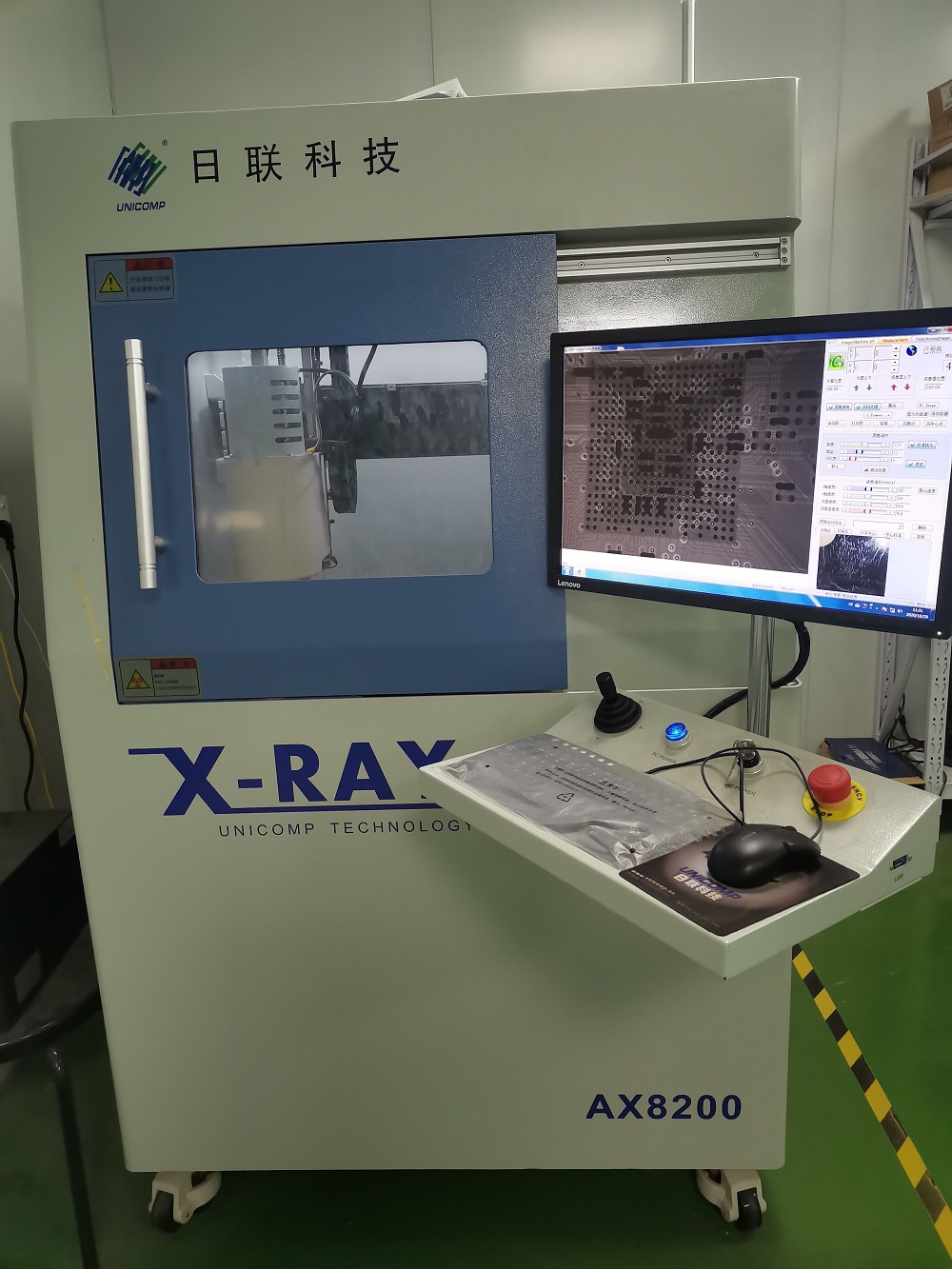
Our BGA assembly lines feature real-time X-ray inspection systems capable of identifying voids smaller than 25% of the pad area, bridging faults, and collapsed ball formations. For industries like industrial control and communications, this ensures robust hidden interconnects where traditional surface inspection methods cannot reach.
BGA rework stations with micro-alignment optics support high-quality repairability when necessary, extending board yield rates beyond 98% even on complex multilayer designs.
| Specification | PCBA Capability |
|---|---|
| Placer speed | 600,000 chips/hour |
| Lead Time | 25+ Days (To Be confirmed) |
| SMT | SMT, Through Hole Assembly Single/Double-Side SMT, Single/Double-Sides Mixture Assembly |
| PCB Size | 50mm×50mm ~610mm×508mm |
| PCB Thickness | 0.5mm~4.5mm |
| Min. diameter /space of BGA | 0.2mm/0.35mm |
| Qualifications | ISO 9001:2015 |
| Accuracy | <±30µm, under the condition of 3σ,CPK≥1 |
| Minimum width/space of QFP | 0.15mm/0.25mm |
| Minimum Diameter /Space of BGA | 0.2mm/0.35mm |
| Reliability Test | Flying Probe Test/Fixture test, Impedance Test, Solderability Test, Thermal Shock Test, Hole Resistance Test, and Micor Metallographic Section Analysis, etc. |
Inline automatic optical inspection (AOI) captures high-resolution 2D and 3D imagery to detect missing components, tombstoning, skew, and insufficient solder joints with a detection accuracy exceeding 95%.
Post-assembly functional testing verifies power integrity, I/O response, and operational logic, helping clients in critical fields like medical monitoring and telecommunications validate every board before final shipment.
OurPCB handles full BOM sourcing through authorized distributors, ensuring traceability down to date and lot codes for critical parts. For hard-to-find electronic components or end-of-life risks, our sourcing teams propose form-fit-function alternatives with full client approval workflows, maintaining compliance with IPC standards and safeguarding continuity in low-mid volume production and scaling phases.
Custom ICT and functional test fixtures are designed in-house to match specific board layouts, providing up to 500 test points for comprehensive validation. Fixture-guided testing reduces operator variability, improves first-pass yield rates by up to 10%, and accelerates fault isolation, a sizable advantage when scaling from prototype quantities into sustained mid volume PCB assembly runs.
OurPCB’s engineering team reviews design files for manufacturability (DFM) and testability (DFT) before production begins, identifying potential assembly challenges such as insufficient solder mask clearance, improper via-in-pad designs, or risky BGA ball layouts. Early correction through DFM/DFT analysis helps clients avoid costly field failures and supports IPC-A-610 Class 2 or Class 3 compliance from the outset.
Detailed BOM reviews are conducted to flag lifecycle risks, sourcing bottlenecks, and component obsolescence. For hard-to-find components or long-lead items, OurPCB develops validated alternative sourcing strategies, protecting the project schedule and maintaining consistent quality standards during mid-volume production scaling.
We allocate specific high-efficiency assembly lines for mid-volume printed circuit board assembly services, maintaining constant process parameters for repeatability. SMT placement tolerances of ±40μm and real-time SPI and AOI monitoring preserve product quality across hundreds to thousands of units without variability, supporting industries where reliability over production volume is non-negotiable.
OurPCB uses Statistical Process Control (SPC) at every critical assembly stage, including solder paste deposition, pick and place accuracy, and thermal profiling. For example, SPI data triggers alerts if paste volume deviates more than 10% from baseline, preventing common failure modes such as cold joints or solder voids before reflow.
A digital production management system ties every work order to specific material batches, operator records, inspection logs, and test results. Customers receive full traceability reports as part of project closure documentation, helping meet regulatory needs in fields such as automotive, aerospace, and medical devices.
OurPCB offers full turnkey PCB assembly services or partial-turnkey models where customers provide free-issue parts. In turnkey engagements, we manage the complete chain from PCB fabrication to final inspection, including sourcing, assembly, testing, and packaging, minimizing coordination risks and ensuring complete alignment with project delivery schedules.
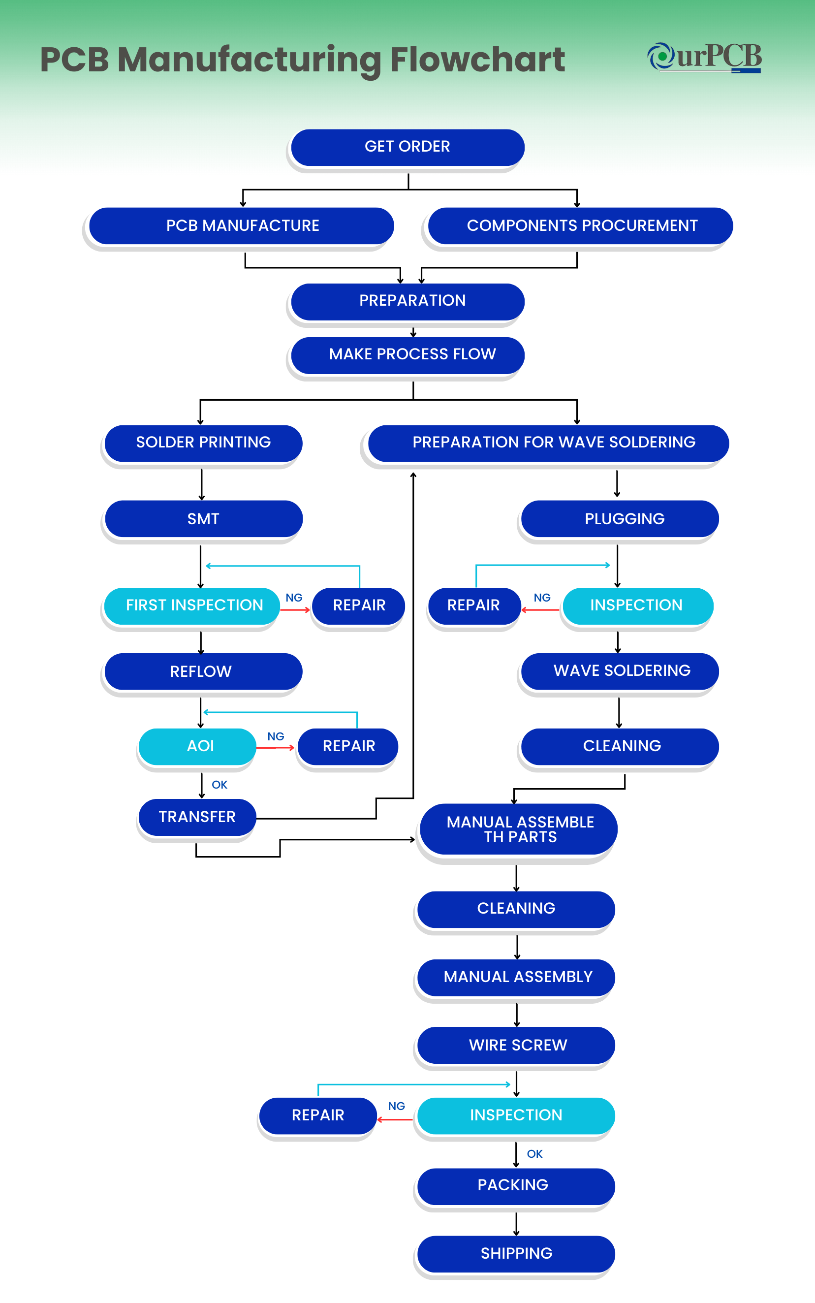
Mid-volume production begins with internal PCB fabrication, where printed circuit boards are manufactured to precise Gerber specifications, often incorporating controlled impedance, blind/buried vias, or HDI features for complex designs.
Material selection, such as FR4, Rogers, or polyimide, is verified, and moisture-sensitive boards are stored in drying cabinets under strict humidity control to prevent delamination or popcorning defects during assembly.
Custom laser-cut stencils are created based on pad design and solder volume calculations.
Solder paste is applied using automated printers equipped with 2D paste inspection systems, followed by SPI measurements checking paste height, volume, and offset tolerances within ±10%.
Early misalignment detection at this stage prevents underfill defects and opens in fine-pitch assemblies.
Components as small as, 01005 packages and fine-pitch BGAs are placed using high-speed pick and place machines, achieving positional accuracy within ±40μm.
Boards then enter nitrogen-assisted reflow ovens, where optimized profiles minimize voiding and thermal stress, particularly important for high-density assemblies in industrial controls and medical monitors.
For mixed-technology boards, through-hole components are inserted manually or robotically, depending on production volume and part size.
Selective soldering machines apply precisely directed molten solder, maintaining thermal integrity for adjacent SMT components and preventing bridging issues common in dense connector regions.
After soldering, inline AOI systems perform 2D/3D inspections checking for tombstones, bridges, open joints, and polarity errors with >95% detection accuracy.
Boards then move through aqueous or semi-aqueous cleaning systems to eliminate flux residues.
If required, selective conformal coating protects circuits against moisture, dust, and chemical exposure, which is necessary for outdoor electronics and automotive modules.
Assemblies undergo functional testing using custom-designed fixtures, verifying I/O functionality, power distribution, and timing stability under real-world loads.
X-ray analysis detects hidden solder defects under BGAs and other bottom-terminated components, achieving void detection sensitivity below 25% pad area per IPC-A-610 guidelines.
Final visual inspection under microscopes confirms cosmetic quality before protective packaging and shipment.
Solder paste deposits are checked using SPI systems that measure height, volume, and pad coverage before placement begins.
OurPCB maintains ±10% tolerance thresholds on solder volume to prevent defects like head-in-pillow and insufficient wetting during reflow.
Early-stage inspection ensures that only boards meeting print quality standards continue through the assembly process.
After reflow, automatic optical inspection scans each board to detect missing parts, polarity errors, tombstoning, skew, and solder bridging.
OurPCB uses both 2D and 3D AOI, allowing volumetric analysis of solder fillets and component seating alongside surface visual checks.
Inspection data feeds directly into production traceability records for real-time yield monitoring.
BGA, CSP, and QFN components are validated through x-ray inspection to uncover hidden defects.
OurPCB’s systems can detect voids occupying over 25% of a pad, collapsed balls, and bridging beneath large packages.
This process meets IPC-A-610 Class 2 and Class 3 acceptance criteria, supporting industries like medical and industrial control, where connection reliability is highly important.
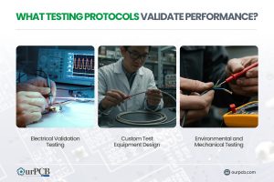
Functional testing and in-circuit testing (ICT) validate the operational behavior and electrical connectivity of completed boards.
Custom test fixtures allow verification of power rails, I/O lines, clock stability, and analog signals under simulated load conditions.
ICT checks shorts, opens, incorrect part placements, and component values down to resistor tolerance levels, improving first-pass yields.
SPC techniques are applied across paste deposition, placement accuracy, reflow profiling, and inspection results to track performance trends. Units passing final optical checks undergo microscope-based verification, confirming cosmetic quality against IPC visual standards. Full traceability of assembly data supports quality reporting for sectors requiring regulatory compliance.
OurPCB operates under ISO 9001:2015 and IATF 16949:2016 certified management systems, with all PCB assembly work conforming to IPC-A-610 Class 2 and Class 3 standards.
Certification-driven process control ensures that mid-volume production maintains mechanical strength, solder joint integrity, and long-term electrical performance even in mission-critical applications.
Our Shijiazhuang and Shenzhen facilities are equipped with high-speed SMT assembly lines, precision stencil printers, selective soldering machines, 3D SPI and AOI systems, and real-time X-ray inspection stations.
Placement accuracy of ±40μm, void detection sensitivity below 25% pad area, and inline SPC monitoring, provide measurable manufacturing reliability across every production run.
OurPCB offers complete turnkey PCB assembly and partial turnkey models, covering PCB fabrication, full BOM sourcing, electronic assembly, inline testing, and logistics support.
Clients can choose flexible service packages that optimize costs, protect supply chains, and meet fast delivery requirements without compromising quality assurance.
We handle full BOM management, sourcing components only from authorized distributors such as Mouser, Digi-Key, Future Electronics, and WPG Holdings.
Special attention is given to long lead-time parts and hard-to-find components, ensuring stable material supply for mid-volume and low-mid volume production orders, without disruptions or last-minute substitutions.
Our quoting system delivers comprehensive pricing for bare PCB fabrication within 8 working hours and mid-volume PCB assembly service quotes within 2 business days after BOM submission.
Internal scheduling flexibility, combined with real-time production management system oversight, supports fast turnaround times with low production risk and predictable project delivery dates.
Since 2007, OurPCB has delivered over 3,000 successful assembly projects across industrial controls, automotive systems, medical devices, and communication infrastructure.
Experience managing both prototype transitions and low-mid volume production provides the technical discipline necessary to minimize ramp-up risks and maintain consistent product quality at scale.
Mon-Fri: 24 hours,
Sat: 9am-6pm, GMT+8
Reach us at
[email protected]
24 hours online
+86-199-30589219
Mon-Fri: 24 hours,
Sat: 9am-6pm, GMT+8
We manufacture PCB assemblies ranging from 50 mm x 50 mm modules to panels up to 610 mm x 508 mm, supporting 1 to 50-layer stack-ups. Controlled impedance, HDI structures, blind and buried vias, and mixed-material builds are available for mid-volume runs, meeting technical requirements across sectors like medical imaging, automotive sensors, and industrial automation.
Yes, OurPCB configures hybrid SMT and through-hole assembly lines to support mixed-technology designs. Boards combining 0201 SMT parts, connectors, and power components up to 20A ratings are processed using selective soldering with nitrogen atmospheres, preventing thermal stress and improving mechanical stability for mission-critical applications.
Solder paste deposition is verified with 3D SPI systems within ±10% volume tolerance, followed by real-time AOI and X-ray inspections after reflow. SPC techniques track variation trends, triggering process adjustments before defects propagate. These controls maintain first-pass yields above 98% across mid-volume production batches.
Every PCB assembly passes inline automatic optical inspection and receives functional testing with programmable fixtures simulating operational conditions. For boards with complex or hidden interconnections, in-circuit testing (ICT) and 3D X-ray verification are applied. Testing strategies are customized based on application criticality, regulatory needs, and expected operating environments.
Yes, OurPCB offers prototype PCB assembly services with the same certified processes used for full production. Early-stage builds benefit from DFM and DFT analysis, allowing clients to identify manufacturability or testability risks before ramping into low-mid volume production. Seamless scaling reduces project lead times and stabilizes quality performance across volumes.
OurPCB delivers complete mid volume PCB assembly manufacturer solutions with full technical control, traceability, and production scalability for your next project.
When considering the best places for manufacturing data cables, China immediately comes to mind. It’s no surprise either — the country has rapidly ascended in
Finding the right wiring harness manufacturer for your vintage ride can be a real headache. Those beautiful old machines need special wiring that looks period-correct
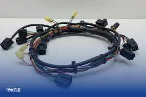
Would your car be able to run without wire harnesses? Not a chance. Wire harnesses connect all the electrical parts together. No harness means no
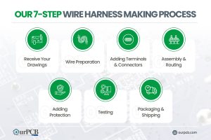
Making wire harnesses isn’t complicated. At OurPCB, we create custom wire harnesses for an expansive range of industries every day. While it’s a complicated process,
Prototype cable assemblies are the very important place in between PCB design ideas and interconnects. OurPCB brings prototype assemblies with PCB solutions to your tables.
PCB thermal management prevents component overheating through strategic heat transfer techniques. Without proper thermal control, electronics are at risk of electronic failures through weakened solder
We use cookies to improve your browsing experience, which may include personal information. By clicking "Agree," you accept our Privacy Policy and cookie use. You can change your cookie settings in your browser anytime.
Agree
 Chat With Us
 Free Quote