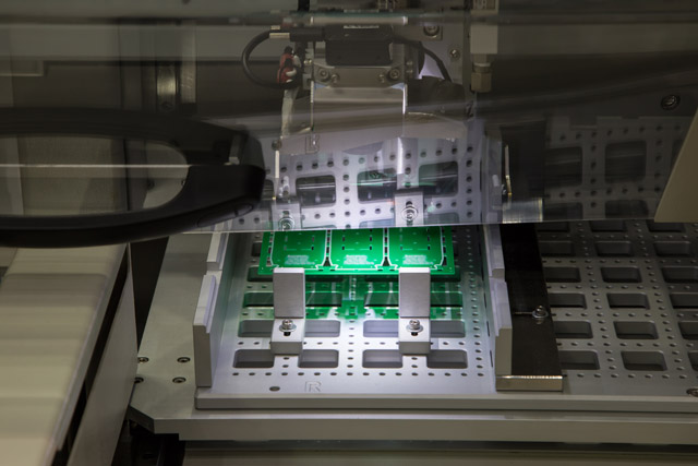
PCB thermal management prevents component overheating through strategic heat transfer techniques. Without proper thermal control, electronics are at risk of electronic failures through weakened solder joints, material delamination, and signal distortion.
Effective solutions for thermal management include wider traces, thicker copper layers, thermal vias, strategic component placement, and appropriate cooling methods based on the PCB’s power requirements. Engineers must select materials with optimal thermal conductivity, from standard FR-4 to high-performance aluminum, copper, or ceramic substrates, to ensure reliable operation in challenging environments.
A properly designed PCB stack-up with conductive paths for heat dissipation maintains performance while preventing thermal cycling damage. Ensure your next design performs reliably under thermal stress. Contact OurPCB’s experienced team for comprehensive solutions tailored to your application needs.
Contents
- What is PCB Thermal Management?
- Why is PCB Thermal Management Important?
- What Causes Heat Generation in a PCB?
- How does Heat Transfer Through a Circuit Board?
- Conduction
- Convection
- Radiation
- When Should PCB Designers use Thermal Simulation?
- What Tools Help You Model Thermal Behavior in PCB Design?
- What Design Techniques Improve PCB Thermal Management?
- Wider Traces and Thicker Copper Improve Heat Transfer
- Thermal Vias and Arrays Reduce Thermal Resistance
- Component Layout Affects Heat Spreading
- Use of Ground Planes and Copper Pours
- Thermal Interface Materials Improve Conduction to Heatsinks
- What are Thermal Vias in PCB Design?
- How Should You Design Thermal Vias?
- Where Should You Place Thermal Vias on a PCB?
- What Cooling Methods Can Be Used to Remove Heat?
- Passive vs. Active Cooling Methods
- Heat Sinks for Passive Heat Removal
- Cooling Fans for Forced Convection
- Peltier Devices for Thermoelectric Cooling
- What Materials Offer Better Thermal Conductivity in PCBs?
- How does PCB Stack-Up Design Affect Heat Dissipation?
- How does Thermal Stress Affect PCB Reliability Over Time?
- What is the Best Cooling Strategy for Each PCB Use Case?
- PCB Thermal Management FAQs
- What are the benefits of metal core PCBs for thermal management?
- Are there industry standards for PCB thermal reliability?
- Can you use metal core PCBs in multilayer designs?
- How does thermal management improve signal integrity in high-speed PCBs?
What is PCB Thermal Management?
PCB thermal management is the process of controlling heat generated by components on a printed circuit board to prevent localized overheating. It directs heat transfer through the board using thermal vias, copper planes, and thermal interface materials, each selected to minimize thermal resistance.
The system relies on design techniques that distribute heat across the PCB surface and guide it toward passive or active dissipation paths. This includes managing all three modes of heat transfer, conduction, convection, and radiation, based on the board's layout and surrounding conditions.
By applying defined PCB thermal management techniques, engineers maintain consistent performance in high thermal dissipation environments while preserving the structural and electrical stability of the circuit board.
Why is PCB Thermal Management Important?
Excess internal temperatures reduce circuit reliability, increase failure rates, and distort signal behavior across the printed circuit board.
Thermal loads from high current devices, such as MOSFETs, IGBTs, and processors, create sharp gradients across the PCB surface. These gradients induce mechanical stress from mismatched thermal expansion rates, weaken solder joints through thermal cycling, and cause delamination in PCB materials with poor thermal conductivities.
Over 55% of electronic failures are directly linked to thermal issues, often from uncontrolled heat generated during continuous operation. Without precise control of the length of the thermal path, localized heating exceeds material thresholds and causes irreversible damage.
Maintaining low thermal resistance through targeted PCB thermal management techniques ensures consistent signal propagation, extends component lifespan, and allows high-density assemblies to meet reliability requirements.
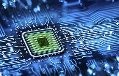
What Causes Heat Generation in a PCB?
Heat in a printed circuit board is caused by resistive losses in traces, vias, and solder joints, along with internal inefficiencies in switching regulators, power ICs, magnetic components, and high-frequency circuitry.
As high current flows through copper conductors, resistance converts electrical energy into thermal energy following the I²R equation. Narrow trace widths, long routing paths, and insufficient copper thickness increase resistance and raise thermal resistance across the circuit board.
For example, a 1-oz copper trace on an external layer carrying 5 amps over 150 mm with a 200-mil width has approximately 0.014 ohms of resistance and produces 0.35 watts of localized heat.
Switching devices and magnetic elements generate heat through core losses and eddy currents, especially under high-frequency operation. In compact PCB designs, these combined effects create thermal hotspots and uneven thermal distribution, making early application of PCB thermal management techniques essential for safe operation and stable PCB performance.
How does Heat Transfer Through a Circuit Board?

Heat in a circuit board moves through conduction, convection, and radiation, with conduction and convection carrying most of the thermal load in standard PCB thermal management applications.
Conduction
Conduction is the dominant mode of heat transfer in PCB design, moving heat through copper and substrate layers from internal heat sources.
When heat from components flows into thermal pads, copper pours, and internal layers, the conductivity of each material determines how efficiently heat spreads. Copper provides high thermal conductivity at roughly 385 W/m·K, while standard PCB materials like FR-4 are far lower, typically between 0.2 and 0.5 W/m·K.
This difference in conductivity creates thermal bottlenecks if heat is not routed through optimized paths. To reduce the length of the thermal path, engineers place thermal vias below heat-intensive packages, often in the form of a thermal via array.
These create vertical conduction channels that move heat into internal planes or opposite board surfaces, supporting low thermal resistance and better thermal distribution across the PCB surface.
Convection
Convection removes heat in PCB assemblies by moving it from the board's surface into ambient air through natural or forced airflow.
In passive heat systems, natural convection carries rising air away from the circuit board, but its effectiveness depends on board orientation and open space. For higher thermal dissipation rates, cooling fans or ducted airflow increase velocity and volume, improving surface cooling.
Effective convection depends on component height, airflow paths, and thermal interface materials like pads or pastes to improve contact with heat sinks. These features expand the surface area for heat dissipation, reduce thermal buildup, and maintain reliable operation in dense layouts.
Radiation
Radiation transfers energy from the PCB surface as infrared waves, contributing a small portion of total heat loss.
While less effective than conduction or convection under standard conditions, radiation becomes more important in sealed enclosures, vacuum environments, or high-temperature LED PCB thermal management applications. Materials with high emissivity and optimized surface geometry improve radiative heat transfer when other methods are limited.
When Should PCB Designers use Thermal Simulation?
Thermal simulation should be used during the early stages of PCB design to identify thermal hotspots, evaluate cooling strategies, and verify that component temperatures remain within safe limits.
When working with high current, dense layouts, or power components that generate significant heat in PCB structures, simulation helps predict how heat will flow through the board and whether heat dissipation is sufficient. This is important when there are limited options for convection, minimal airflow, or constrained board area.
Designers should also run simulations using thermal vias, heat sinks, or thermal interface materials to model their effectiveness and confirm overall thermal resistance. These models allow teams to visualize thermal distribution, optimize the length of the thermal path, and test multiple layouts without costly physical prototypes.
By applying simulation before fabrication, PCB designers can reduce field failures, shorten development cycles, and improve thermal performance in high-power or space-constrained circuit board assemblies.
What Tools Help You Model Thermal Behavior in PCB Design?

Thermal analysis software tools like Ansys Icepak, Simcenter Flotherm, COMSOL Multiphysics, and PCB-Investigator Physics model thermal behavior in PCB design.
These tools simulate heat transfer through conduction, convection, and radiation by processing layout geometry, copper distribution, and component power data. They identify thermal hotspots, calculate thermal resistance, and visualize thermal distribution across the printed circuit board.
Each tool can evaluate heat generation from power components, test thermal vias and thermal interface materials, and optimize heat sink design based on airflow and stack-up structure.
While open-source options like Elmer and Calculix support basic analysis, commercial thermal analysis tools offer the precision required for dependable PCB thermal management.
What Design Techniques Improve PCB Thermal Management?
Wider traces, thicker copper, thermal vias, ground planes, and optimized component placement are the most effective design techniques for improving thermal management in PCBs.
These methods reduce localized heating, lower overall thermal resistance, and increase the board’s capacity to dissipate heat from high-power components. Each PCB thermal management technique enhances heat transfer through improved conduction paths or by expanding the surface area for heat dissipation, supporting long-term reliability and stable electrical performance.
Wider Traces and Thicker Copper Improve Heat Transfer
Widening copper traces and increasing copper thickness reduces I²R losses and improves heat transfer capacity in PCB designs. Moving from 1 oz (35 μm) to 2 oz (70 μm) copper can double the current-carrying capability while cutting trace resistance in half.
A 250-mil trace of 2 oz copper can safely carry over 10 amps with a temperature rise under 20°C, supporting higher thermal dissipation along the trace. Wide traces, when combined with large copper pours, increase the surface area for heat dissipation, minimizing hotspots across the PCB surface.
Thermal Vias and Arrays Reduce Thermal Resistance
Thermal vias act as vertical conduction paths, connecting hot components on the surface to internal or bottom copper planes. A typical via has a diameter of 0.3 mm and is spaced 0.8 to 1.0 mm apart in a thermal via array.
Filling and capping these vias with copper or conductive epoxy improves reliability and blocks solder wicking under large thermal pads. Dense arrays reduce the length of the thermal path and help achieve low thermal resistance between the component and external heat sinks, especially when used under power ICs or regulators.
Component Layout Affects Heat Spreading
Component placement plays a direct role in thermal distribution. High-power devices like MOSFETs, LED drivers, and regulators should be positioned near board centerlines to allow radial heat flow. Avoid clustering multiple heat sources in a confined region.
Instead, distribute them evenly across the circuit board and align them with active or passive airflow regions. Keep a minimum spacing of 2 to 3 mm between high-dissipation parts and avoid placing them near sensitive analog components or connectors prone to thermal drift.
Use of Ground Planes and Copper Pours
Unbroken internal and external ground planes are thermal conductors, spreading heat from components horizontally across the board. Connecting these planes to thermal vias under ICs creates a combined lateral and vertical heat transfer system.
For optimal thermal conductivity, use solid copper layers with at least 70% coverage and ensure thermal relief connections are minimized or avoided near power sections. Multilayer PCB designs benefit from staggered copper pours on alternating layers to distribute thermal loading more uniformly.
Thermal Interface Materials Improve Conduction to Heatsinks
Thermal interface materials (TIMs) such as thermal pads, phase-change compounds, or silicone pastes bridge the microscopic gaps between components and heat sinks, reducing boundary resistance.
TIMs with thermal conductivities above 3 W/m·K are recommended for applications exceeding 3 W of heat generation per component. Proper pressure during mounting (typically 20 to 50 psi) ensures full surface contact and uniform thermal performance. Without these materials, trapped air gaps significantly degrade heat dissipation efficiency and raise interface temperatures by 10 to 20 °C.
Special Offer: Get $100 off your order!
Email [email protected] to get started!
What are Thermal Vias in PCB Design?
Thermal vias are plated through holes and are strategically used in PCB thermal management to move heat from surface-mounted components into internal or bottom copper layers.
They are filled with copper and conduct heat vertically through the board by linking the thermal solder pad of a component to larger copper areas. This design allows thermal energy to flow away from the component, improving the board’s ability to transfer heat through conduction.
How Should You Design Thermal Vias?
Design thermal vias by maximizing vertical conduction from the thermal solder pad to internal or bottom copper layers using properly sized, tightly spaced, and well-positioned plated holes.
Start with thermal via diameters between 0.2 mm and 0.4 mm, which balance thermal conductivity with manufacturability. Arrange vias in a uniform grid with 0.8 mm to 1.0 mm center-to-center spacing, and increase the via count based on power dissipation. For components generating 2 to 5 watts, use 8 to 16 vias directly beneath the package footprint to support effective heat dissipation.
Connect each via to large copper areas on inner or opposite layers to reduce thermal bottlenecks and improve the board’s ability to transfer heat. Where solder control is needed, fill vias with epoxy and cap them with copper to prevent wicking during reflow.
These practices are standard in high-power PCB thermal design and represent proven PCB design techniques for reducing the thermal resistance between active components and surrounding structures.
Where Should You Place Thermal Vias on a PCB?
Thermal vias should be placed beneath heat-generating components and connected to copper planes on internal or bottom layers that absorb and spread thermal energy efficiently.
Position the vias directly under the thermal solder pad, where heat concentration is most significant, and connect them to uninterrupted ground or power planes to form a low-resistance conduction path.
In multilayer stacks, select inner layers with minimal signal density to avoid interference between thermal conduction paths and electrical routing.
Avoid placing thermal vias near high-speed signal lines or analog circuits sensitive to temperature variation or structural disruption. Where airflow or heat sinks are present, shift via placement closer to those features to shorten the conduction path to the cooling interface.
In compact layouts, innovative PCB thermal management involves grouping thermal vias into defined thermal zones that control local heating without impacting critical circuit behavior.
What Cooling Methods Can Be Used to Remove Heat?
Cooling methods in PCB thermal management are divided into passive and active types, depending on whether they rely on natural conduction or powered mechanisms to remove heat.
Passive methods use copper planes, thermal vias, and heat sinks to move thermal energy without electrical input. Active methods apply forced airflow or thermoelectric devices to extract heat in high-power or enclosed systems.
The method chosen depends on layout density, airflow availability, and the total heat generation expected under load.
Passive vs. Active Cooling Methods
Passive cooling uses conduction and natural convection through copper pours, planes, and thermal vias to move heat without powered elements. Active cooling adds cooling fans or thermoelectric modules to accelerate heat transfer in high-power or confined assemblies.
Heat Sinks for Passive Heat Removal
Heat sinks increase the surface area for heat dissipation and lower junction temperatures by up to 30 °C in natural airflow. Attach them to components over copper planes or materials with high thermal conductivity to improve passive thermal conduction.
Cooling Fans for Forced Convection
Cooling fans force airflow across the PCB surface, improving convective cooling by 30–50%. A 40 mm axial fan at 6000 RPM provides up to 15 CFM, reducing thermal buildup near power devices and PCB layouts with poor natural ventilation.
Peltier Devices for Thermoelectric Cooling
Peltier devices use current to pump heat away from components. Modules rated for 10–100 W require a heat sink on the hot side and thermal contact with the cold side. These are used for local cooling in dense or high-precision PCB designs.
What Materials Offer Better Thermal Conductivity in PCBs?
Materials with higher thermal conductivity improve a printed circuit board’s ability to move heat away from components and maintain stable temperatures.
Substrate selection directly affects PCB thermal design, especially in applications with high heat generation or limited airflow. While FR-4 remains the industry standard for general-purpose use, alternatives like aluminum, copper, and ceramic are used when effective heat dissipation and lower thermal resistance are necessary for reliable operation.
| Material Type | Thermal Conductivity (W/m·K) | Typical Use Cases | Advantages | Limitations |
|---|---|---|---|---|
| FR-4 (Glass-Reinforced Epoxy) | 0.2 to 0.5 | Low-power consumer electronics, general-purpose digital PCBs. | Inexpensive, easy to fabricate Dielectric constant (Dk) ≈ 4.2, widely supported by fab shops | Poor heat transfer High thermal resistance Mismatched CTE to ceramic packages |
| Aluminum (Metal Core PCB) | 1.0 to 3.0 | LED drivers, compact power supplies, and automotive ECUs. | Integrated thermal plane Mechanical rigidity Supports thermal vias, CTE ≈ 23 ppm/°C | Limited to 1 to 2 signal layers Requires a dielectric bonding layer (20 to 100 μm) Testricted routing |
| Copper Substrate | 4.0 to 6.0 | RF amplifiers, heavy-current industrial control boards. | Excellent heat dissipation Low impedance power delivery Minimal thermal lag | High cost Weight penalty Differential CTE with top layers Complex multilayer integration |
| Aluminum Nitride (Ceramic) | 150 to 180 | Space-grade sensors, laser drivers, mmWave radar modules. | Very low dielectric loss, Dk ≈ 8.5 High breakdown voltage, CTE ≈ 4.5 ppm/°C (close to silicon) | Fragile under mechanical shock High per-unit cost Tight process tolerances |
| Beryllium Oxide (Ceramic) | 250 to 285 | Defense microwave assemblies, high-power optoelectronics, pulsed RF systems. | Highest thermal conductivity for PCB substrates Dk ≈ 6.7, strong electrical isolation | Toxic when machined, strictly regulated Expensive Unsuitable for standard PCB fab infrastructure |
How does PCB Stack-Up Design Affect Heat Dissipation?
PCB stack-up determines the path heat takes through copper layers and dielectric materials, directly influencing how thermal energy spreads and exits the board.
Layer arrangement, copper plane placement, and dielectric thickness control the board’s internal thermal flow and define how effectively it conducts heat away from active components. These structural choices also affect overall thermal resistance and how the board responds to thermal cycling during operation.
How does Thermal Stress Affect PCB Reliability Over Time?
Thermal stress weakens a circuit board by causing mechanical fatigue, material expansion mismatch, and interconnect failure during repeated temperature cycling.
As the board heats and cools, copper, laminate, and solder joints expand at different rates, generating internal strain. This leads to cracking, delamination, solder fatigue, and eventual electrical failure.
High layer counts, large BGA packages, and mismatched CTEs increase vulnerability. Over time, even minor thermal effects can accumulate and compromise long-term PCB reliability, especially in high-power or harsh-environment applications.
What is the Best Cooling Strategy for Each PCB Use Case?
The best cooling method for a PCB depends on power, airflow, and environmental stress.
Higher power or tighter spaces require active solutions, while larger boards with lower thermal loads may use passive conduction.
| Use Case | Recommended Cooling Strategy | Power Range | Temperature Range | Thermal Design Reasoning |
|---|---|---|---|---|
| Low Power, Large Board | Copper planes + thermal vias | < 10 W | Ambient: 32 to 122 °F (0 to 50 °C) | Copper pours spread heat laterally; thermal vias conduct vertically to cooler layers. No active parts needed for proper thermal management. |
| Medium Power, Low Airflow | IMS + heat sink design + thermal pad | 10 to 30 W | Junction: 140 to 212 °F (60 to 100 °C) | IMS provides a 1.0 to 3.0 W/m·K thermal path; the heat sink increases the radiating area; the pad fills interface gaps. Ideal where airflow is restricted. |
| High Power, Tight Space | Heat pipe + fan + thermal pad | 30 to 100 W | Junction: 212 to 257 °F (100 to 125 °C) | Heat pipes move >100 W from dense zones; fan delivers forced convection; pad reduces contact resistance. Best for compact, high-density heat management. |
| Harsh Environment | Ceramic PCB + thermal encapsulant | 20 to 80 W | Ambient: –40 to 185 °F (–40 to 85 °C) | AlN (≈180 W/m·K) or BeO (≈250 W/m·K) supports a wide delta-T. Encapsulant prevents delamination and corrosion from moisture, vibration, or thermal cycling. |
Request your free quote, and we’ll ensure that your PCB matches the thermal requirements you’ve outlined. We offer material compatibility confirmation and process flow for your next PCB assembly in under 24 hours, so you can match your deadlines with time to spare.
PCB Thermal Management FAQs
What are the benefits of metal core PCBs for thermal management?
Metal core PCBs (MCPCBs) use an aluminum or copper base to provide faster heat transfer and lower thermal resistance than standard FR-4.
These boards are ideal for PCB thermal management in high-power LED lighting, motor controllers, and power converters, where heat must be extracted through the base layer quickly. The metal substrate also improves mechanical stability and reduces thermal cycling fatigue.
Are there industry standards for PCB thermal reliability?
Yes, IPC-2221 and IPC-2152 define guidelines for thermal via usage, trace width vs. current capacity, and temperature rise limits. MIL-STD-202 covers thermal cycling and shock reliability testing. These standards ensure that PCB thermal design supports long-term electrical and structural integrity under load.
Can you use metal core PCBs in multilayer designs?
Yes, but with constraints. Most MCPCBs are single- or double-sided due to the metal core's isolation requirements. However, hybrid builds combine a metal base layer with multiple signal layers using prepregs or dielectric adhesives. These designs offer the best heat path while preserving moderate signal routing flexibility.
How does thermal management improve signal integrity in high-speed PCBs?
Lower board temperatures reduce dielectric loss, control impedance drift, and minimize timing variation in high-speed designs. Effective heat dissipation stabilizes material properties, especially in RF, DDR, and SerDes interfaces. Thermal control also reduces outgassing, which affects conformal coating and long-term insulation resistance.
Back to Top: PCB Thermal Management | Effective Cooling & Heat Management
Special Offer: Get $100 off your order!
Email [email protected] to get started!