
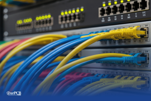
Top 7 Truck Wiring Harness Manufacturers
Truck wiring harnesses are the electrical backbone of commercial vehicles, from long-haul trucks to construction fleets and emergency vehicles. They must withstand continuous vibration, thermal

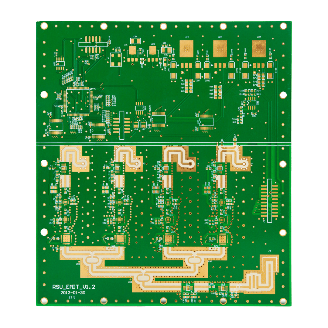
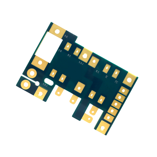
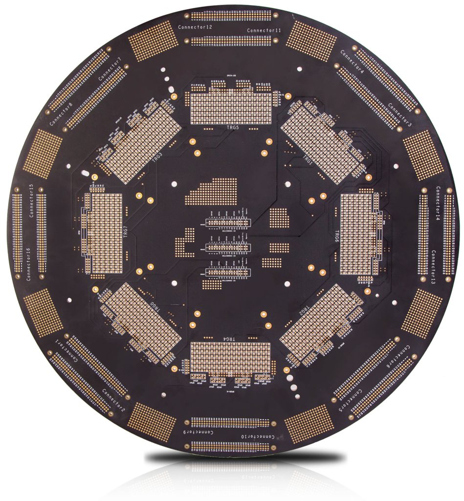
At OurPCB, we deliver exceptional bare PCB manufacturing services with advanced capabilities, rigorous testing protocols, and industry-leading quality standards. Our state-of-the-art facilities in China manufacture high-quality bare printed circuit boards that combine cutting-edge technology with decades of fabrication expertise. Whether you need bare circuit boards for prototypes or production, our bare board PCB manufacturing meets the most demanding specifications for electronic projects across all industries.


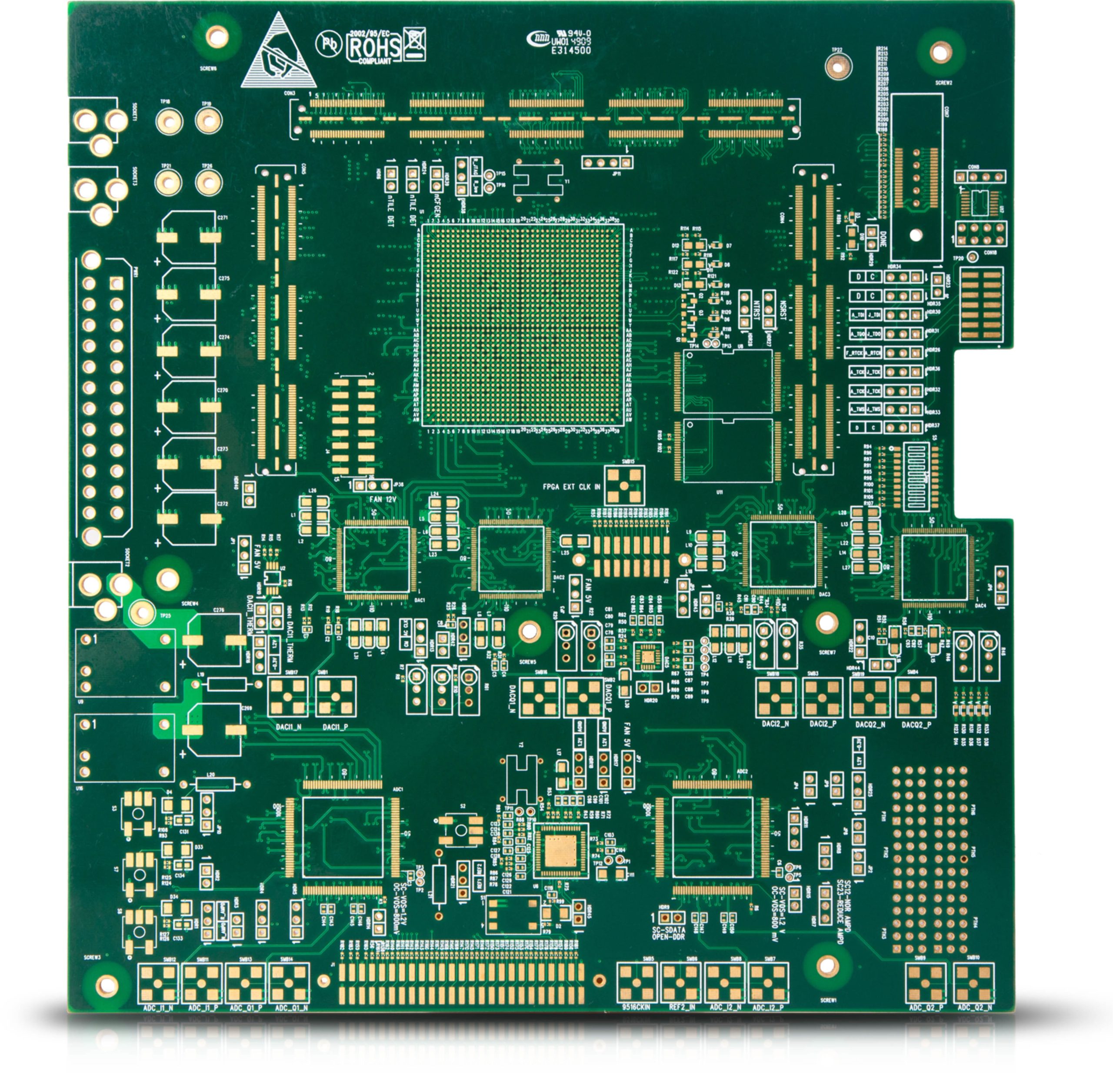

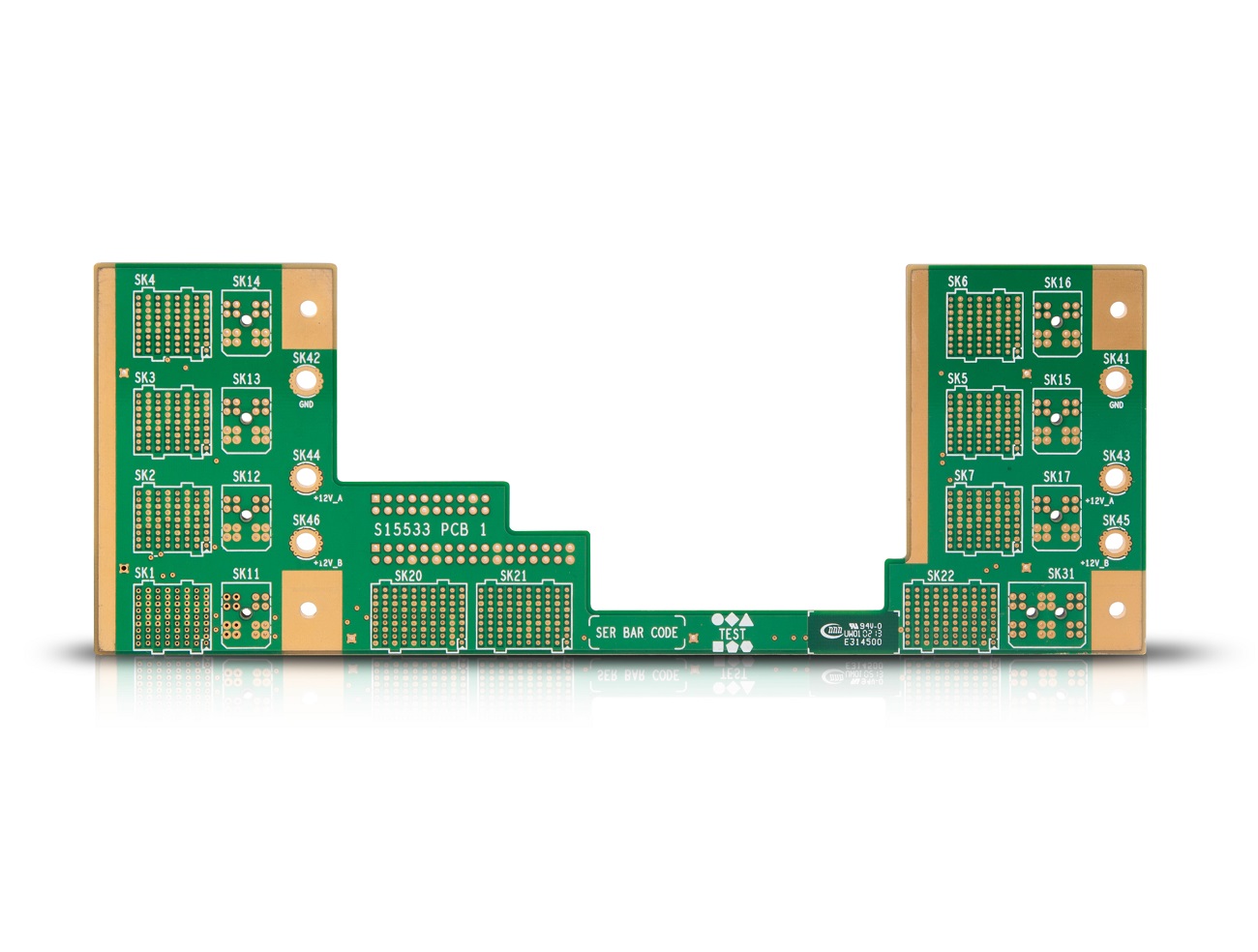
Bare PCB boards are printed circuit boards without any electronic components, consisting of substrate material, conductive copper pathways, and protective coatings that form the foundation of all electronic devices. These essential bare boards direct electrical current through precisely designed pathways while providing mechanical support for the assembly process. The quality of bare PCBs directly determines the reliability, performance, and longevity of finished electronic products.
Our bare circuit board manufacturing process incorporates stringent quality controls at every stage, from initial design verification through final inspection, ensuring PCBs that meet exact specifications. We utilize advanced materials including high-temperature FR-4, Rogers, and specialized ceramics to support applications ranging from consumer electronics to medical devices and aerospace systems.


Our bare PCB board manufacturing delivers exceptional value through precision engineering, comprehensive testing, advanced materials, and manufacturing expertise. As a leading bare PCB manufacturer, these benefits translate directly to improved product performance, reliability, and speed to market for your electronic projects.

OurPCB has been a top bare circuit board manufacturer since 1986, delivering superior bare board fabrication through our combination of advanced technology, rigorous quality systems, exceptional technical expertise, and comprehensive service offerings. As bare PCB suppliers, we focus on every detail to ensure perfect performance in your application. In a market projected to grow at 3% CAGR through 2030, we maintain competitive advantage through innovation and quality that exceeds the industry average first-pass yield of 92%.

OurPCB delivers an extensive suite of PCB assembly solutions, tailored to accommodate a variety of project requirements. We focus on delivering accuracy, efficiency, and stringent quality control throughout every stage of the assembly process.
We specialize in Surface Mount Technology (SMT) assembly, ideal for devices that demand compactness and high performance. Utilizing advanced pick-and-place equipment, we achieve highly accurate placement of components, ensuring reliable and consistent results.
We provide adaptable assembly models to suit your preferences. You may supply your own components for assembly, or choose our comprehensive turnkey service, where we manage component sourcing, assembly, and logistics from start to finish.
Our custom assembly services are designed to accommodate your specific designs, including intricate layouts and unique requirements. Our team collaborates closely with you to ensure all project specifications are fulfilled to your satisfaction.
We offer expedited PCB assembly services, delivering finished boards rapidly without compromising on quality. Even under tight timelines, we adhere to rigorous quality standards to ensure reliable performance.
We manufacture assemblies that comply with IPC Class 3 standards, which are essential for applications in sectors such as aerospace and medical devices. These assemblies are engineered for the highest levels of reliability in demanding environments.
Our capabilities extend to the precise assembly of all integrated circuit (IC) package types, including BGAs, POPs, CGAs, QFNs, DFNs, and CSPs. Our state-of-the-art equipment allows us to handle even the most complex IC packages with confidence and accuracy.
OurPCB employs a meticulous eight-step bare PCB manufacturing process that integrates quality assurance at every stage. Our process begins with comprehensive design file analysis using advanced DFM tools that identify and resolve potential issues before production starts. This approach prevents downstream manufacturing problems and ensures higher first-pass yields for your bare copper board.
Material selection critically impacts bare printed circuit performance, reliability, and application suitability. Our bare PCB factories offer an extensive range of substrate materials to meet specific project requirements, from standard FR-4 to specialized high-frequency laminates for multilayer PCBs.
| Material Type | Properties | Recommended Applications |
|---|---|---|
| FR-4 | Tg 130-140 °C, Good electrical properties | General electronics, Consumer devices |
| High-Tg FR-4 | Tg 170-180 °C, Enhanced thermal stability | Industrial controls, Automotive systems |
| Rogers | Low dielectric loss, Excellent RF performance | High-frequency applications, Microwave circuits |
| Polyimide | Extreme temperature resistance, Flexibility | Aerospace, Defense systems, Flexible circuits |
| Aluminum-backed | Enhanced thermal dissipation | Power electronics, LED lighting, Motor controls |
Impedance control is critical for high-speed digital and RF applications where signal integrity determines performance. As experienced bare PCB manufacturing suppliers, we implement precise impedance control through specialized material selection, careful stackup design, and manufacturing process controls. We achieve controlled impedance with ±10% tolerance across all board layers for circuit board prototypes and production runs.
Our bare PCB manufacturing manufacturer status is built on comprehensive testing methodologies that verify both physical and electrical characteristics of every bare board. Our testing approach combines automated optical inspection with advanced electrical testing to ensure perfect compliance with design specifications for printed circuit board fabrication. We exceed standard IPC-6012 requirements by implementing IPC-A-600 Class 3 acceptance criteria, and our quality assurance laboratory maintains NIST-traceable calibration for all measurement equipment.
Our comprehensive testing protocol includes additional verification methods like X-ray inspection for multilayer registration and impedance testing using calibrated TDR systems that detect variations as small as 2%.
OurPCB’s fabrication services deliver exceptional technical capabilities that surpass industry standards. Our advanced technology includes CNC drilling that achieves precise hole placement with ±0.001″ accuracy, while our laser drilling systems create microvias as small as 0.004″ for high-density interconnect applications.
| Capability | Specification | Advantage |
|---|---|---|
| Maximum Layers | From 2 layers up to 8-layer and beyond | Supports complex, high-density designs |
| Board Manufacturing | 0.2 mm to 7.0 mm thickness | Accommodates diverse application requirements |
| Minimum Trace/Space | 0.0762 mm/0.0762 mm (3mil/3mil) | Enables surface mount technology solutions |
| Standard PCBs | Multiple sizes available | Ideal for most electronic components |
| Maximum Aspect Ratio | 12:1 | Superior plating process for thick boards |
| Surface Finishes | HASL, ENIG, Immersion silver, OSP, Hard gold, Soft gold | Optimal solutions for different solder requirements |
Contact us today to discuss your bare PCB manufacturing requirements and get a quote. Our technical experts will review your design specifications and recommend the optimal manufacturing approach for your project. With OurPCB as your bare printed circuit board supplier, you’ll receive precision-engineered products and services that provide the perfect foundation for your electronic products.
Request a quote online for your next PCB orders or call our technical sales team to begin your bare PCB manufacturing project with the best product for your needs.
Mon-Fri: 24 hours,
Sat: 9am-6pm, GMT+8
Reach us at
[email protected]
24 hours online
+86-199-30589219
Mon-Fri: 24 hours,
Sat: 9am-6pm, GMT+8
HASL (Hot Air Solder Leveling) applies molten solder to copper surfaces, providing good solderability at lower cost but with less planarity, while ENIG (Electroless Nickel Immersion Gold)deposits nickel and gold layers that offer excellent flatness for fine-pitch components and extended shelf life.
Blind vias connect an outer layer to one or more inner layers without extending through the entire board, while buried vias connect only internal layers without reaching the surface. These specialized via structures differ from standard through-holes by enabling higher routing density and improved signal integrity in complex multilayer designs, though they require more sophisticated manufacturing processes involving sequential lamination.
Bare printed circuit board turn time depends primarily on board complexity, layer count, and material availability, with each factor influencing production scheduling and processing time. High layer counts require multiple lamination cycles, special materials may have extended procurement times, and complex designs demand additional setup and testing procedures, though expedited fabrication services can accelerate delivery for time-critical projects.
Truck wiring harnesses are the electrical backbone of commercial vehicles, from long-haul trucks to construction fleets and emergency vehicles. They must withstand continuous vibration, thermal

Medical cable assemblies sit at the intersection of electrical safety, biocompatibility, and sterilization durability. For regulated medical devices, OEMs must work with manufacturers that understand
Robotics cable assemblies are unlike ordinary cables, they must survive continuous motion, tight bend radii, torsion, vibration, electrical noise, and often harsh industrial or outdoor
Waterproof cable assemblies have to do more than just “keep water out.” For outdoor, marine, industrial washdown, and transportation platforms, assemblies are expected to survive
Aerospace cable assembly manufacturers work under standards such as AS9100, ISO 9001, and RTCA/DO-160, and many also maintain ITAR registration to support flight-critical and space-qualified
When considering the best places for manufacturing data cables, China immediately comes to mind. It’s no surprise either — the country has rapidly ascended in
We use cookies to improve your browsing experience, which may include personal information. By clicking "Agree," you accept our Privacy Policy and cookie use. You can change your cookie settings in your browser anytime.
Agree Chat With Us
 Free Quote