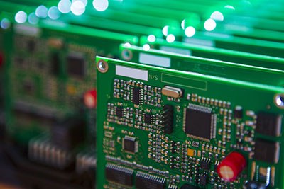
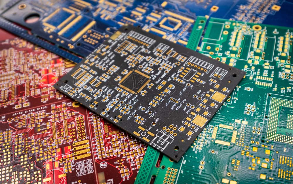
Assembling a board with hundreds of components can be an expensive and complex process that consumes a lot of time. Therefore, it is necessary to ensure the underlying printed wiring board functions optimally before assembly to avoid costly board-level repair. Bare printed circuit board gives you a blank platform that you can test before assembly to avoid these expensive repairs. We will look at these PCBs to analyze their benefits from an electronics production standpoint. Let's get right into it!
Contents
- What is a Bare Printed Circuit Board?
- Bare PCB vs. Zero PCB: What’s The Difference?
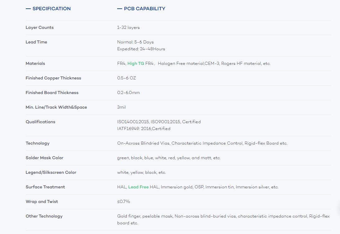
- Bare Printed Circuit Board Capabilities
- Why Use a Bare Board?
- When To Use a Bare Board
- Advantages of Bare Boards
- Early Defect Detection
- Saves Time
- Cost Saving
- Materials Used For Bare PCB Manufacturing
- FR4
- PTFE
- Metal
- Bare Board Manufacturing Process
- Pre-Production
- Inner-Layer Imaging
- Inner Layer Etching
- Lamination
- PCB Drilling
- Electroless Copper Deposition
- Outer Layer Imaging
- Graphic Plating
- Outer Layer Etching
- Solder Mask Curing
- Surface Finishing
- Electrical Board Testing
- V-Scoring and Profiting
- Visual Inspection
- Possible Errors in Bare PCB Board Manufacturing
- Missing or Excessive Copper
- Short Circuiting
- Extra Holes
- What is Bare PCB Testing?
- Types of Bare Board Testing
- Wrap Up
What is a Bare Printed Circuit Board?
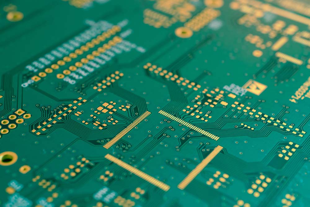
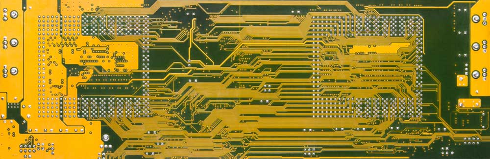
In a nutshell, a bare PCB board is a circuit board without thru-holes or electronic components. It is the skeleton of conventional PCBs and consists of a substrate, conductive pathways, metal coating, and patterns.
A bare-printed circuit board
Some industry experts refer to bare boards as PCBs or blank PCBs, while assembled boards are PCBA.
Bare PCB vs. Zero PCB: What’s The Difference?
Also known as blank PCBs, bare PCBs are unassembled circuit boards. They only have the substrate base with copper traces, solder mask, and silkscreen layers, but no components soldered on the pads.
Therefore, this board only provides the electrical pathways, which you can use for testing purposes. Once you approve of the design, you can assemble the board to handle its specific function.
Several bare PCBs are ready for testing.
But zero PCBs are general-purpose circuit boards; they aren’t built to handle a specific purpose.
So, while the bare PCB is an unchangeable solution, zero PCBs allow you to test the circuit design before finalizing it into a PCB design.
Zero PCBs are also known as perfboards or dot PCBs, where the dots or pads are not connected (unlike breadboards). You must connect the components with wires after inserting them into the holes.
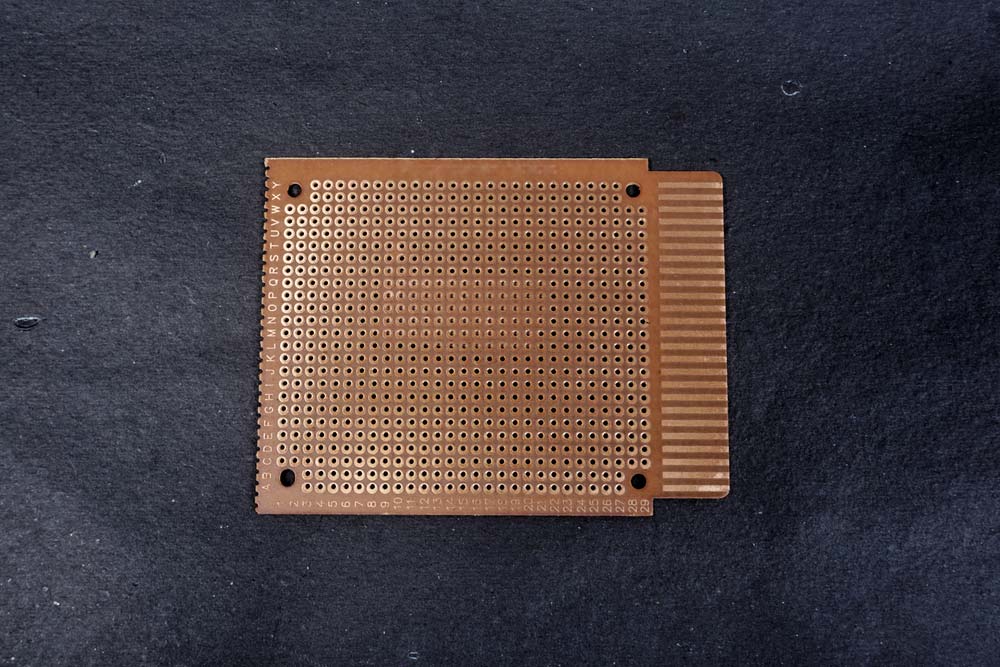
A dot or perforated PCB, which you can use for making and testing electronic circuits.
Bare Printed Circuit Board Capabilities
Why Use a Bare Board?
A bare board is like a skeleton or backbone that forms a frame for customized configuration. Therefore, you can use it to test designs, functionality, and concepts before assembling expensive components.
A bare PCB
The testing process helps eliminate issues that can affect the usability of an electronic device. On top of that, the bare board provides mechanical support to the circuit and electrical components.
Special Offer: Get $100 off your order!
Email [email protected] to get started!
When To Use a Bare Board
Since bare boards are complete, unchangeable solutions, they come after testing the circuit using a zero PCB or breadboard.
Essentially, they are the circuit only and consist of copper traces, not wires. Therefore, you should use them when testing the circuit prototype.
The purpose of testing the circuit is to identify any shortcomings that can affect the device’s performance before mounting the expensive components.
Remember, you had tested the circuit earlier on the zero PCB or breadboard using wires.
But in the actual PCB, factors like noise interference and parasitic capacitance can affect the circuit’s performance because the traces are positioned close to each other.
A bare PCB with gold-plated pads for the components and IC.
So, you must test the circuit board as a prototype before going into mass production.
You might have to go through several bare board iterations as you refine the product before coming up with the best design.
After that, you can mount the components, do the final test, then mass-produce the board.
Advantages of Bare Boards
Besides mechanical support and creating a compact circuit for testing, bare boards have the following advantages.
Early Defect Detection
The bare board's surface does not have electronic parts or other obstructions.
So you can examine their design and structure to detect any issues with select single components or copper patterns.
It will be cheaper to rectify these issues at this stage than if you encounter them after assembly.
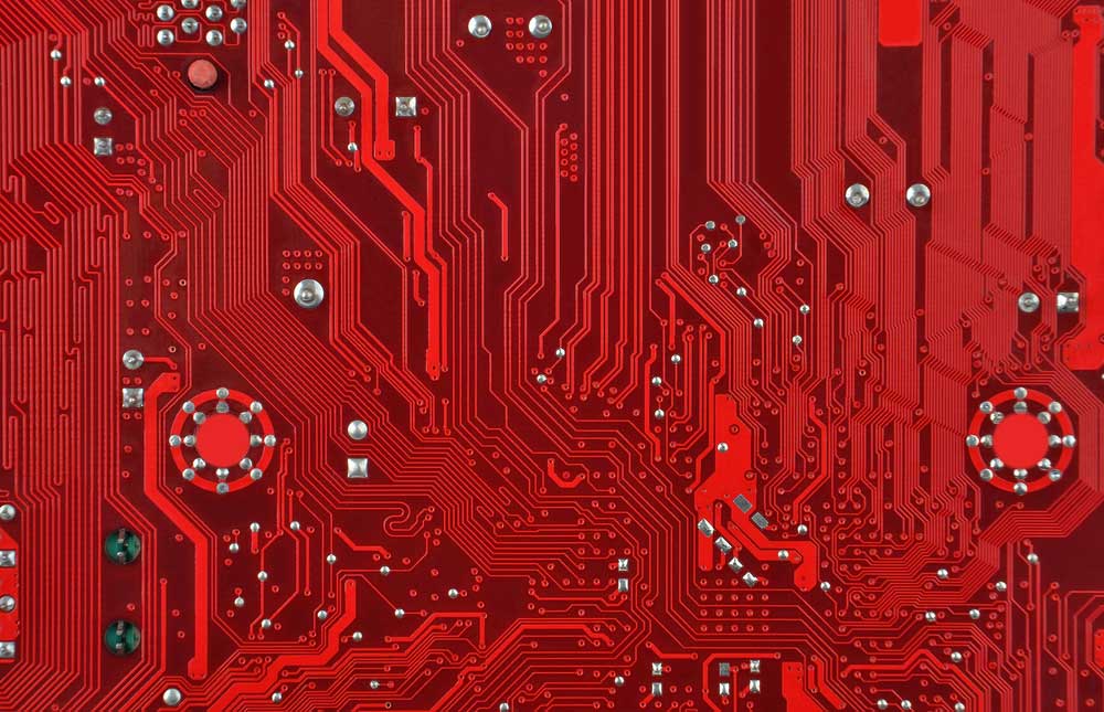
A red-printed circuit board with no components
Saves Time
Early electrical testing and prototyping ensure you achieve design-specific functionality.
So you won't waste time assembling functional components on a faulty PCB.
Cost Saving
Since bare board testing is a foundational process that helps with board design, fabrication, and testing, it ensures the PCB is durable and functional.
Early problem detection is cheaper to fix, so you will minimize losses and possibly avoid damaging expensive components by soldering them to a faulty board.
Also, time is money. So saving time implies you save money.
Materials Used For Bare PCB Manufacturing
The primary section of a bare PCB is the substrate or base layer, and it can consist of any material that is strong enough to hold the traces and components. But the most common ones are FR4, PTFE, and metal.
FR4
FR is an acronym for Flame Retardant, while four refers to a glass-reinforced epoxy resin.
FR4 is like the standard or de facto material for making PCBs because it is relatively affordable, insulative, water resistant, mechanically strong, and fireproof.
PTFE
is the second most popular material for building circuit board substrates because it is costlier than FR4.
However, it performs better because it provides consistent dielectric properties at a higher coefficient of expansion, making it ideal for high-speed, high-frequency boards.
So you’ll most likely encounter this material if handling a microwave bare PCB.
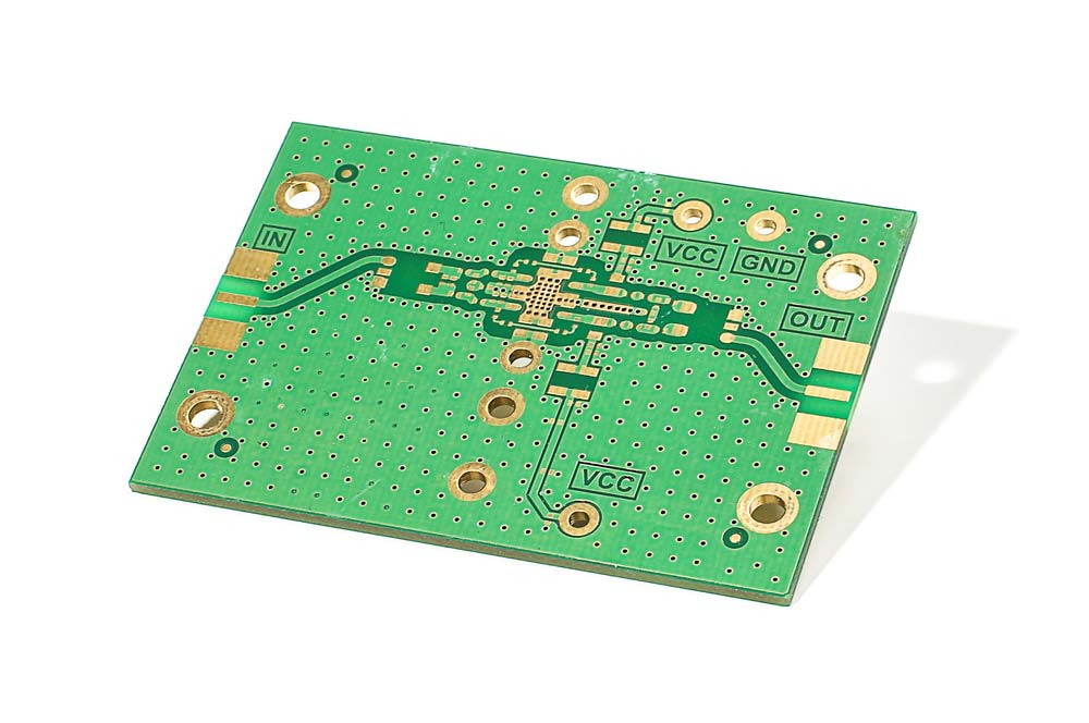
A radio-frequency amplifier PCB with a PTFE or Teflon substrate.
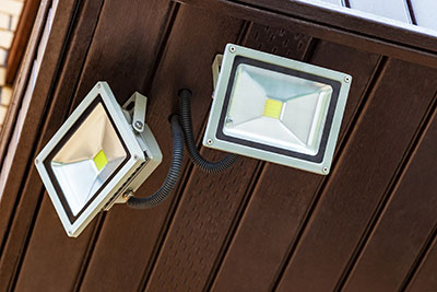
Metal
Metal base PCBs offer high mechanical strength and thermal dissipation.
The second factor is the most important factor here because it is handy when your circuit will have components that emit a lot of heat, such as LEDs.
However, metal is also electrically conductive, so the material should have an insulative coat above the metal.
Bare Board Manufacturing Process
Fabricating bare boards involves the following steps.
Pre-Production
After sending the Gerber design/board layout file to the manufacturer with the production and customization information, the engineers align the specifications and capabilities to ensure compliance.
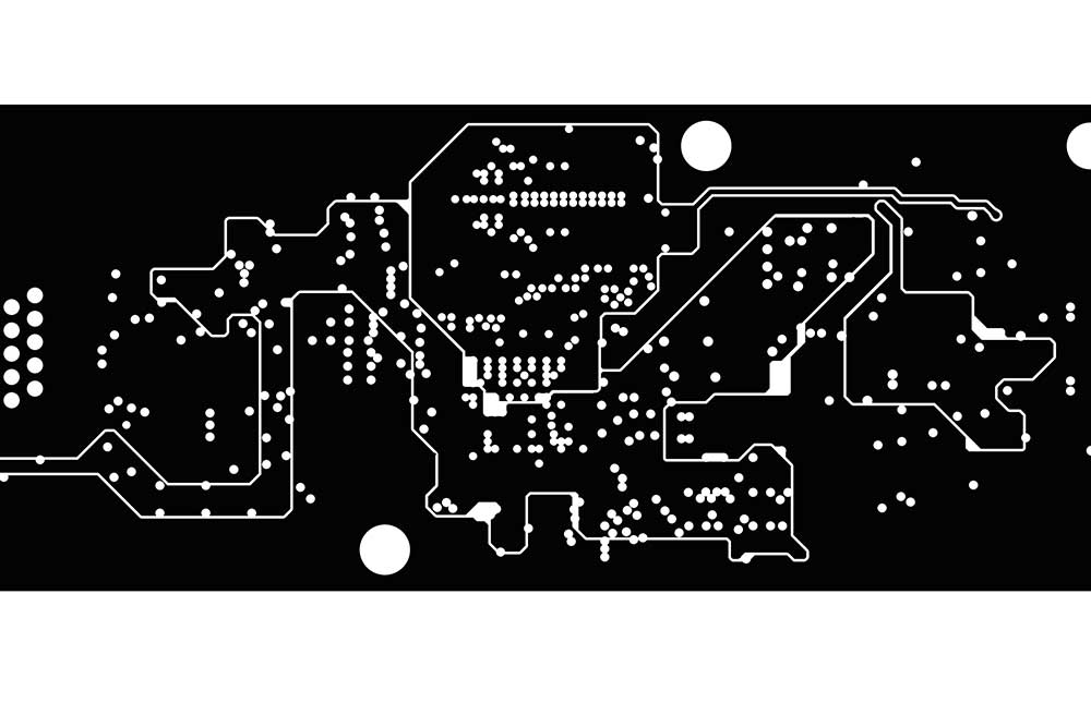
A Gerber file showing the layout of a PCB’s inner layers
Inner-Layer Imaging
A focused laser beam defines the PCB traces into the board directly.
Inner Layer Etching
The etching process removes all excess copper residue from the PCB to ensure the circuitry/copper pattern matches the design.
Lamination
Oxide layers are the most typical printed circuit board laminates. So lamination involves applying an oxide layer to the inner board layer, then stacking them together. The oxide layer acts as insulation in multilayer boards. A copper foil also gets added. But the inner layers require a complete machine inspection before lamination to avoid mistakes.
PCB Drilling
Drilling creates holes that act as electrical connection contacts and optimize layer links.
Electroless Copper Deposition
The next step is electroless copper deposition, which deposits a thin copper layer into the drilled holes. This process conceals the holes and seals the board.
Outer Layer Imaging
This imaging process removes the dry film to ensure the circuit runs as required. After that, additional copper gets plated.
Graphic Plating
This plating process places an extra layer on the dry film parts. After copper deposition, the additional tin plating prevents oxidation for maximum durability.
Outer Layer Etching
Outer layer etching removes the excess copper residue and dry blue film. The tin-metallic plating safeguards the essential copper circuitry components.
Solder Mask Curing
Some sections of the PCB get exposed to UV light, while others get removed. After that, the board undergoes a curing process using a solder mask, which creates a smooth, high-quality finish.
A multilayer PCB with green solder stop mask
Surface Finishing
Surface finishing creates organic or metallic solderable surfaces for surface-mount component placement and soldering.
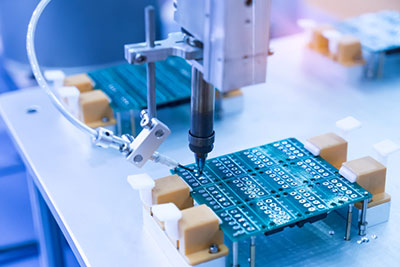
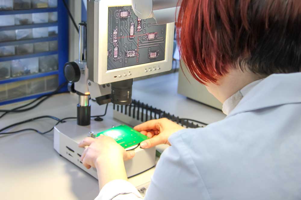
Electrical Board Testing
The board is complete at this point, and the next step is to test if the PCB traces are functional and conduct electric signals as required. You can test the boards using fixture-less testing, flying probe, or universal grid testing.
V-Scoring and Profiting
Production panels get routed into specific shapes and sizes to match the production file. V-scoring involves cutting V grooves on the board's top and bottom for easy layer or component-level separation without damage.
Visual Inspection
The final step is an optical inspection of the entire board by a team of skilled and qualified engineers who check if the board meets the required standards. Once the boards pass the inspection process, they go into packaging and delivery.
An engineer is inspecting a PCB visually.
Possible Errors in Bare PCB Board Manufacturing
Since the bare PCB is a prototype, it can have several defects, which you should identify when testing to improve the structure in the subsequent version.
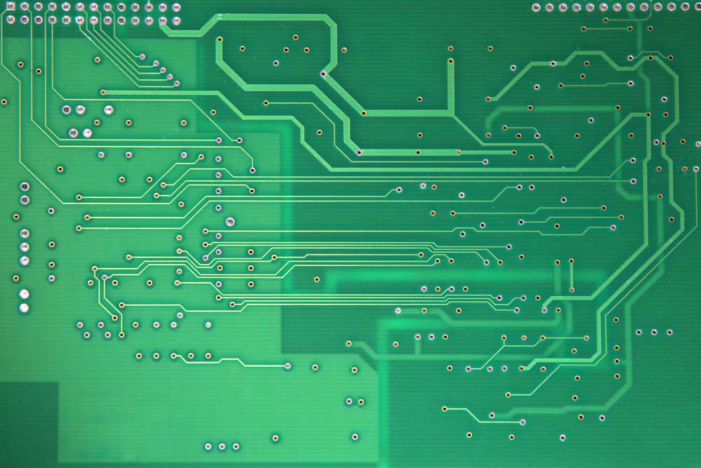
Missing or Excessive Copper
Copper is the electrically conductive material used to make the traces for electricity and signal transmission.
They begin as copper foils that undergo etching using a chemical solution to leave the transmission lines.
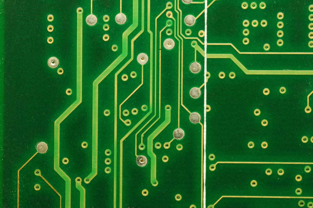
Copper traces and holes (vias) on a blank printed circuit board.
Errors can occur during etching, leaving excessive copper that causes interference or capacitance with the adjacent traces using the thin insulative material in between as the dielectric.
Etching can also deplete sections of the copper traces, resulting in discontinuities.
Short Circuiting
This error can occur if there’s excessive copper in some areas that causes two traces to come into contact.
But the manufacturer can also create erroneous contacts between traces and pads, which causes a short.
During testing, you will notice an abnormally high current flowing through the circuit due to this issue.
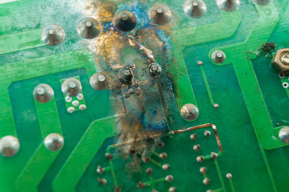
A PCB with a shorted section that has discolored the green solder mask.
Extra Holes
Bare PCBs have through holes and conductive vias, which should be just the right number and all usable.
Excess, unutilized holes can limit the space available for other functions, such as component mounting or signal trace routing.
Eliminating these excesses enables you to optimize the circuit design.
What is Bare PCB Testing?
Bare board testing is the electrical testing done on blank PCBs to evaluate the isolation and continuity of the wiring board connections. Isolation testing checks the resistance between two electrical connections, while continuity testing ensures the circuits don't have open points that can impede current flow.
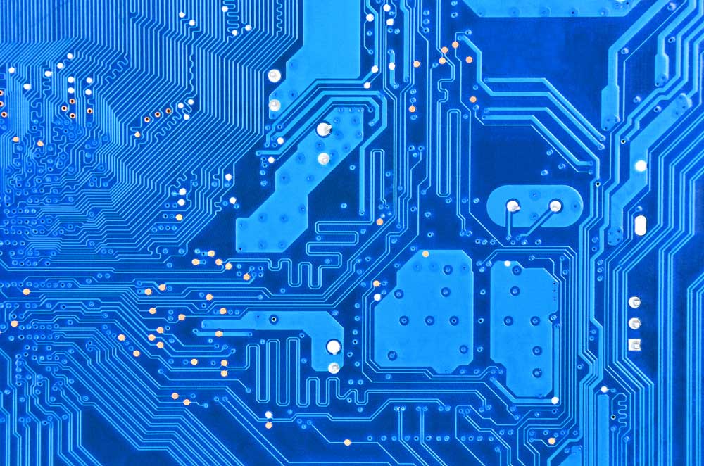
A blue-printed circuit board
Types of Bare Board Testing
The traditional method of testing bare boards is by using a digital multimeter. But the process is not feasible with modern multilayer boards because they are complex.
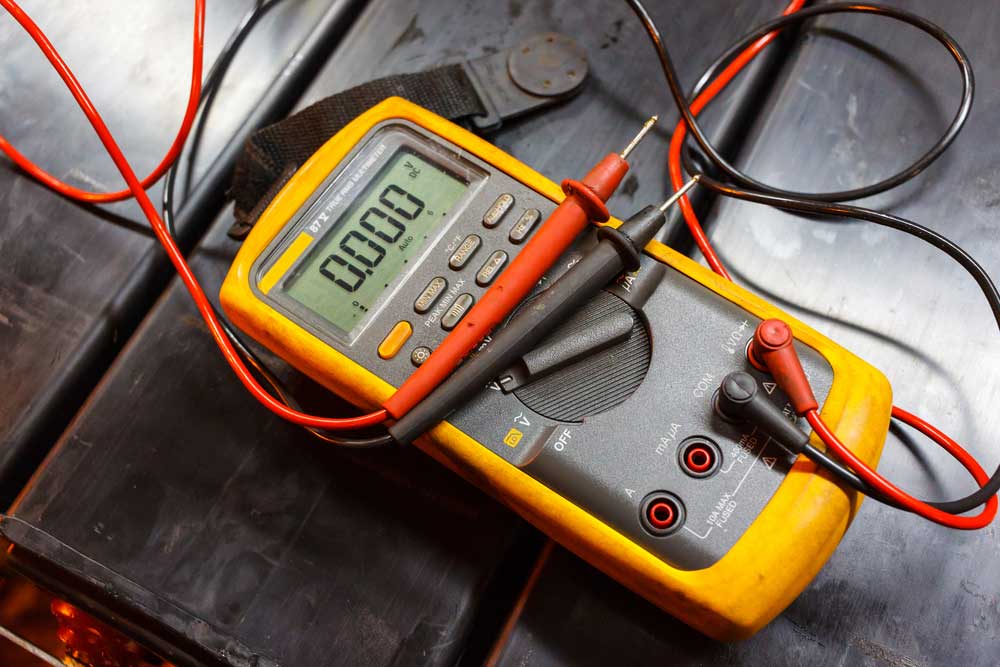
A digital multimeter
So the viable testing methods for modern-day, high-volume production include the following.
- Flying probe test
- Pinned fixture test
- Burn-in test
- Automated optical inspection
- X-ray inspection
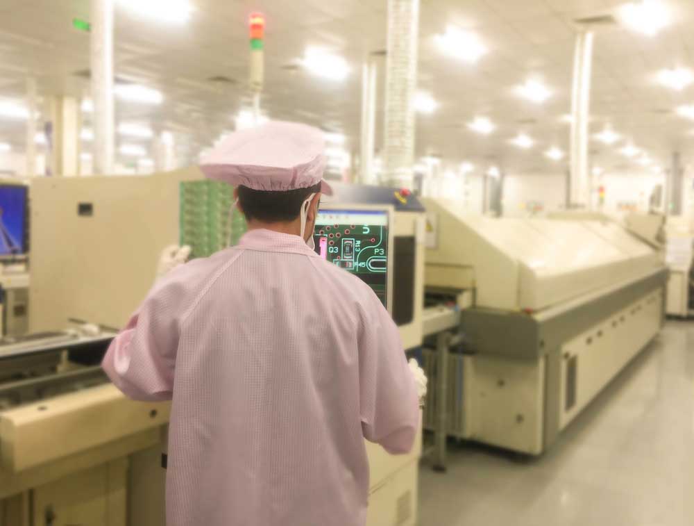
Automated optical inspection of a PCB by a factory worker
Wrap Up
In conclusion, bare printed circuit boards are more viable for the mass production of electronics than unique PCBs because they have the versatility and flexibility advantage.
And we have the experts to help you actualize your board from the design files. Contact us for more details if you want a high-quality PCB or PCBA for your project.
Special Offer: Get $100 off your order!
Email [email protected] to get started!