Another advantage of the modern way of making PCBs is that we have better technology now. Today, we have PCBs, and even though the production processes are not always easy, they can be automated. Special software can even do parts of the work, mainly if the PCBs are produced in large quantities.
So if you are new to the world of printed circuit boards, you are fortunate. This article will learn all crucial things about how PCBs are made, the standard PCB panel size, other PCB panel sizes, and above all, the best company to choose when you want to make printed circuit boards.
As you read on, you will also understand why PCBs have different panel sizes and know how to decide which PCB fabrication panel size is best for your circuit board. This article is the whole package, so pay attention as you read further.
Contents
1、PCB Panel Size
To start making a PCB, the first step is to create a custom printed circuit board. This is because full boards need to be fixed into the panel to be used for production.
Different penalization methods are employed when working on a PCB panel to determine the desired size and function. The most common methods include V-groove and tab route, which is also known as breakaway tab penalization.
Depending on what the manufacturer sees best to reduce cost and improve the circuit board's quality, one of the above methods will penalize aboard. Some manufacturers can go as far as using both v-groove and tab route methods simultaneously on a single project. This combination of methods usually increases the cost of PCB production, but it reduces damages as well, so the extra money is worth it.
Every PCB has a particular reason it is being made, and because these reasons are so diverse, there will undoubtedly be different sizes of printed circuit boards in the market. Electronic designers usually go through tedious processes to ensure they get the maximum number out of aboard. It is tedious, but it is worth the effort and sometimes extra cost when you look at the finished product.
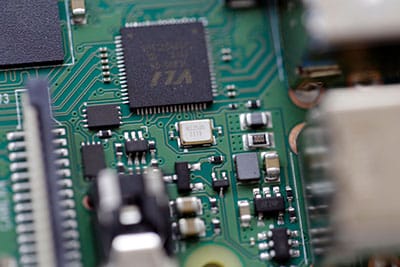
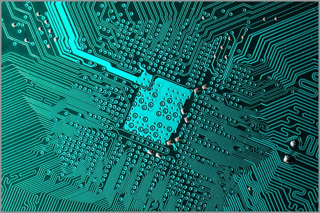
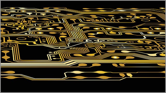
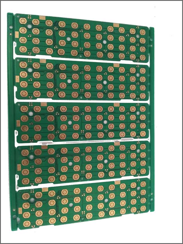 Image 1: PCB Panel Size
We cannot discuss the standard PCB panel size without mentioning the thickness of a circuit board. It is essential to manufacture a circuit board, and if the consistency is not measured correctly, the PCB will not function well if it even functions at all.
As a customer who intends to buy a perfect PCB, you should say where and how the PCB you want to buy will be used.
This information will go a long way to help makers decide how thick the circuit board will be. If you're going to buy more than one PCB, you should also tell your producers the different devices you want each type to work with. This way, the level of thickness for every PCB you get will vary concerning the intended function of the electronic device.
By standard PCB panel size, the thickness of an average circuit board is 0.063inches. To achieve maximum efficiency of a PCB, this size and other preparation steps are put into consideration. The standard PCB panel size is calculated so that a highly efficient utilization area utilization is achieved.
When it comes to efficiency, a lot depends on the method used to separate the individual boards from the array. That involves the [Inserted: at]standard PCB panel size, the clearance between the two adjacent pairs, and other related points.
With efficiency at its maximize, the thickness at its best, and [Inserted: e th]standard PCB panel size put into consideration, it is safe to say that your circuit board will come out perfect for whatever device you want to use it for.
The engineers have to do one other thing when making your printed circuit board is to customize it. Panels are customized with the materials available to the manufacturer of your PCB, but if you want specific features, make sure you inform your manufacturer. It may cost you more, but the output will be worth every penny you spend.
The circuit layout of your printed circuit board does not have to be identical. Depending on what you want and what your manufacturer feels is best for your device, some variations may be done to the layout, but that is not something you should worry about since efficiency is not affected.
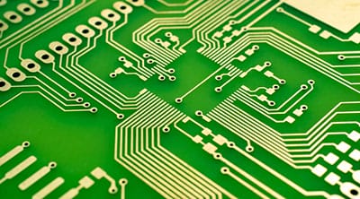
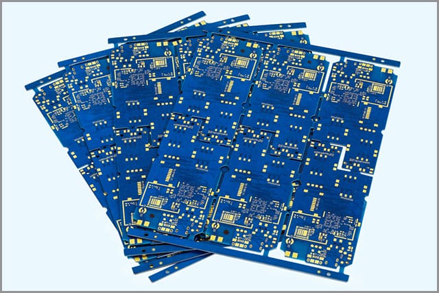
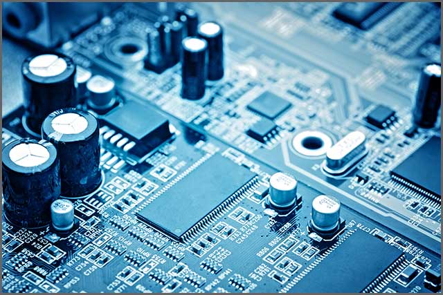 Image 2: Standard PCB Panel
Special Offer: Get $100 off your order!
Email sales@ourpcb.net to get started!
2、Standard PCB Panel Size
We cannot discuss the standard PCB panel size without mentioning the thickness of a circuit board. It is essential to manufacture a circuit board, and if the consistency is not measured correctly, the PCB will not function well if it even functions at all.
As a customer who intends to buy a perfect PCB, you should say where and how the PCB you want to buy will be used. This information will go a long way to help makers decide how thick the circuit board will be. If you're going to buy more than one PCB, you should also tell your producers the different devices you want each type to work with. This way, the level of thickness for every PCB you get will vary concerning the intended function of the electronic device.
By standard PCB panel size, the thickness of an average circuit board is 0.063inches. To achieve maximum efficiency of a PCB, this size and other preparation steps are put into consideration. The standard PCB panel size is calculated so that a highly efficient utilization area utilization is achieved.
When it comes to efficiency, a lot depends on the method used to separate the individual boards from the array.
That involves the [Inserted: at]standard PCB panel size, the clearance between the two adjacent pairs, and other related points.
With efficiency at its maximize, the thickness at its best, and standard PCB panel size is put into consideration, it is safe to say that your circuit board will come out perfect for whatever device you want to use it for.
The engineers have to do one other thing when making your printed circuit board is to customize it. Panels are customized with the materials available to the manufacturer of your PCB, but if you want specific features, make sure you inform your manufacturer. It may cost you more, but the output will be worth every penny you spend.
The circuit layout of your printed circuit board does not have to be identical. Depending on what you want and what your manufacturer feels is best for your device, some variations may be done to the layout, but that is not something you should worry about since efficiency is not affected.
Standard pcb panel size
3、PCB Panel Standard Size
In PCB manufacturing, specific special tools are used to enhance the effectiveness of the random circuit boards. These tools are advanced computer analytics tools, and they are made to work correctly with the standard PCB panel size.[Deleted:c][Deleted:rta][Deleted:n][Deleted:pe][Deleted:f]
Also, the number of layouts on the standard PCB panel size plays a role in determining how effective the board turns out to be. The higher the number of forms, the more influential the printed circuit board will be.
To make it more transparent, let me use an example. If a 16 by 22 inches circuit board panel size fits a two six by 9 inches layout, the efficiency will be up to about 80 percent. Looking at a different scenario, if a standard PCB panel size is matched with two six by 5 inches layouts, the efficiency will be at a discouragingly low 30 percent.
The idea is to keep an average ratio between the standard PCB panel size and the circuit design layout. If you use a big panel size and dissect it into a large number of smaller formats, the result will be terrible, as the efficiency will fall.
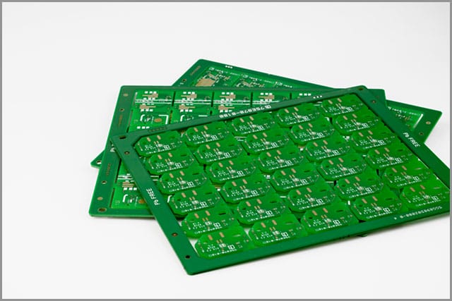
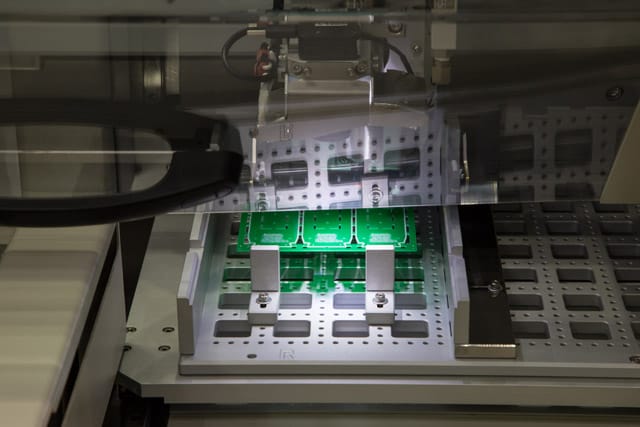 Image 4: Standard PCB Panel Size
While still working with the standard PCB panel size, factors like the method of penalization a manufacturer decides to use and other points will affect the efficiency of a PCB device.
It is not that manufacturers of PCBs can't choose to use other dimensions for the circuit boards, they definitely can, but most of them decide to use the standard PCB panel size because of reasons like cost. The entire production process consumes less money when the standard PCB panel size is used.
Still, on the standard PCB panel size, there is also the issue of configuration.
Most producers of PCBs do not make their panel size because the standard PCB panel size is easy to configure; it is like the designing and assembling are automated, so it is less work for them.
Smaller devices usually require corresponding small circuit boards. So if you happen to need a PCB for a small device, the good news is that there may not be a need for penalization. For example, if you use a two by 2 circuit board panel size, there won't be a need for penalization, which means the cost of producing that circuit board will reduce.
It takes us back to the point I mentioned earlier in this article about letting your manufacturer know what you want to do with the PCB you want to buy. It makes it easier for you to have the most suitable circuit board for your device and help you save some money, like in this case, where penalization is not necessary.
4、PCB Fabrication Panel Size
When a printed circuit board is constructed, using the standard PCB panel size makes work lighter and faster. Remember the two most used methods of PCB penalization we talked about pointed out in chapter one? They both have different reactions to the fabrication panel size of a circuit board. By this, I mean their efficiencies vary concerning the PCB size.
For a standard PCB panel size of 18 by 24 inches, the border clearance needed would not be more than half inches. When the layers increase, the border clearance required also grows with it, so half inches will no longer be sufficient for a standard PCB panel size with multiple layers.
Clearance for the handling and alignment marks takes up considerably large space in the standard PCB panel size.
In the 18 by 12 inches board, it is common for 16 by 10 inches to be filled with the layout. However, multilayer boards require additional marking and assembly clearance.
No matter what method is being used during penalization, both border clearance, milling clearance, and specific routing are essential. When you need similar boards to be produced, it is much faster and costs less to make, but when you need different circuit boards to be manufactured for various purposes, the process becomes more challenging.
When making circuit boards that are not for the same purpose, the penalization process will prove tedious no matter which method is used. Only skilled and experienced professional Engineers can carry out this task and make something good out of it.
Usually, the extra skill associated with the production of the printed circuit board is because of the characteristic automation that is missing. Most identical standard PCB panel size boards are easy to configure and penalize, but the strategic positions must be fixed manually when it comes to individually different boards. This is the main reason why you need to patronize only experts when you want to buy printed circuit boards for different purposes.
If you are new to this industry or need to know how to minimize costs when you buy printed circuit boards, be assured that it is not difficult. You need to know about the standard PCB panel size and some other information I will share right now.
By now, you already know that the chief reason why some PCBs cost more than others is that of the circuit board penalization process and the unique needs any board may require. If your proposed circuit board is not the usual type manufacturers get asked to do most times, yours will cost more because it won't need automatic processes to create. More technology, more money.
So what if your broad has special needs?
Do you need to spend so much money? The answer is no, but that depends on your manufacturers because you will need them to cooperate with you as you try to minimize cost and still get the best work done.
Reducing the cost of producing your particular circuit board is all about knowing how to economize the space on your standard PCB panel size. If, for some reason (which will most likely be the unique structure of your proposed circuit board), you happen to settle for a circuit board with dimensions outside that of the standard PCB panel size, make sure you are careful when choosing the fabrication panel size of your PCB.
You can't do this without your manufacturer. So before you choose a PCB fabrication panel size, ask your manufacturers what they think will be best for you. Since they are experts in the industry, they should know the dimensions that will be perfect for the type and purpose of your circuit board.
If you have chosen a high-class PCB manufacturing company like OURPCB Tech, this will not be a problem at all. They will do more than usual by advising you on the size of the PCB fabrication panel you should use for your board and going the extra mile to give you details of the spaces between the circuit boards and the panel edges well.
If your circuit board manufacturing company cannot do these things for you, you should consider leaving them for a more professional company. That will give clear instructions on how your board should be designed for it to be as efficient as possible, no matter how far your proposed board's dimensions may be from the standard PCB panel size.
To avoid having any damage done to your printed circuit board in the course of production, all stress points must have the needed support. Modern assembly lines and fully automated robotic handling keep the PCBs safe even when they are in a high production volume environment.
5、Conclusion
Many points have been made here, with enough emphasis placed on specific areas directly connected to maximizing the efficiency of your printed circuit board. One of those areas of utmost importance is the way you choose a company to manufacture your PCB.
Even if you have much money, get all your PCB fabrication panel size calculations right, and enough time on your hands to check on the company as the work is going on, it does guarantee you an adequate product if you are working with the wrong circuit board manufacturing company!
This is why choosing a manufacturer for your work is by far the most critical aspect of acquiring a PCB.
Let's not forget other apparent reasons like cost, efficiency, integrity, customer service, and many more. So, be wise and choose OURPCB Tech as the company to make your printed circuit board.
As far as reputation goes, OURPCB Tech has impressed customers since 2005. These customers have left excellent reviews for you to see when you search the Internet. Also, OURPCB Tech is certified by top professional bodies in this industry like Printed Circuit Board Industry Certifications, ISO9001 certification, ISO and UL certifications, and a lot more you can see here as proof of high-quality assurance.
No matter your PCB needs, this company will make it happen for you quickly and at a very affordable fee. Reach out to OURPCB Tech today by sending an email to sales@ourpcb.com for the best service and support you need even after buying the PCB.
Special Offer: Get $100 off your order!
Email sales@ourpcb.net to get started!