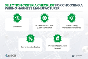
Top 10 Classic Car Wiring Harness Manufacturers | Full Guide
Finding the right wiring harness manufacturer for your vintage ride can be a real headache. Those beautiful old machines need special wiring that looks period-correct

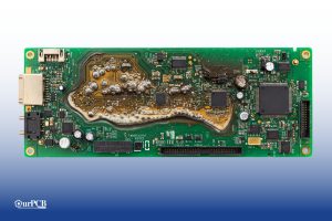
At OurPCB, we manufacture high-quality ceramic PCBs using alumina and aluminum nitride. We serve anyone who needs superior thermal performance, electrical insulation, and long-term durability. Our team delivers consistent quality, fast turnaround, and global shipping—making us the trusted choice for LED, power electronics, and aerospace applications.


A ceramic PCB is a high-performance circuit board made with fine ceramic materials like alumina or aluminum nitride. These materials offer exceptional thermal conductivity, dispersing heat efficiently from hotspots and protecting sensitive components. Ceramic PCBs are manufactured using advanced techniques like Laser Activation Metallization (LAM), which enables precise and reliable conductor patterns. Their low dielectric loss and mechanical strength make them suitable for high-frequency, high-voltage, and harsh-environment applications. As a result, ceramic PCBs are widely used in power electronics, RF modules, aerospace systems, and LED lighting.


At OurPCB, our ceramic PCBs are in high demand because they deliver outstanding thermal conductivity, electrical insulation, and durability under extreme conditions. Clients across industries choose our boards for their proven reliability in high-power, high-temperature applications like LEDs, aerospace, and power electronics.

The first reason why ceramic boards are so popular in the electronics sector is their excellent thermal coefficient of expansion.
It is good to note that the ceramic base heat transmission almost matches silicon and can act as a connection material. Besides, you can use it as an isolator.
For applications requiring exceptional thermal performance, such as high-temperature PCBs, ceramic boards are indispensable due to their adaptability to adverse conditions.
The application of ceramic brings a stable dielectric capacity, and you can modify the balance into a partial radiofrequency loss to increase your device’s power.
Still, despite the surface roughness, ceramic materials come with an inherent resistance against chemical erosion. Ceramic’s chemical resistance can change to resistance against liquids and moisture.
Integrated metal core boards with high thermal expansion can be used for several applications. Using the sintering technique, the metal core can still be turned into a reliable conductor. Therefore, ceramic PCBs’ high processing temperatures make them beneficial.
The ceramic board fabrication process creates durability through unique properties, such as toughness. That prevents your PCB from wear and tear.
You can be confident that you will not change your PCB soon because of its slow aging capacity. Also, the high thermal resistance of ceramic PCBs makes it assume a decelerated decomposition process.
Lastly, metal cores can serve as inflexible carriers that offer mechanical stiffness. This property makes it easier to use ceramic PCBs in any state of matter because of the high resistance to corrosion and normal wear and tear.
Ceramic is not a single material; it is a group of hard, brittle, corrosion-resistant, and heat-resistant materials that PCB manufacturers can use as the base material.
These fabricators usually pick these ceramics while considering the CTE and thermal conductivity properties, and the most typical ones include the following.
Unlike aluminum, alumina(Al2O3) is a crystalline powder material with high electrical resistivity (about 1 x 10¹⁴Ω.cm ).
The common purity of the material ranges from 94% to 99%, with alpha-phase alumina (over 95% purity) being the strongest and stiffest.
96% alumina is the most common in this range because it is affordable and has a CTE of 4.5 to 10.9 x 10⁻⁶/K thermal conductivity of 25 W/(m.k). For further insights into materials with superior thermal management properties, such as aluminum PCBs, check out this comprehensive guide.
This non-oxide semiconductor has a hexagonal crystal structure and a bluish-white color when 100% pure, but it can be white, gray, or pale yellow when impure.
Aluminum nitride (AlN) is the best substrate material for ceramic PCBs because its thermal conductivity can be as high as 300W/(m.k).
Its electrical resistivity is also better than alumina’s because it ranges from 10 to 16 Ω.m. But it is expensive.
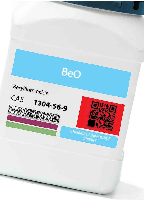
Except diamond, beryllium oxide (BeO) has one of the highest thermal conductivity values of all nonmetals (ranges from 209 to 330W/(m.k)).
Additionally, it has strong, rigid bonds between its atoms that raise its melting and boiling points to 2575°C and 3905°C, while its CTE ranges from 7.4 to 8.9 x 10⁻⁶/K. These properties make it valuable in various electronics and other industries.

Unlike aluminum, alumina(Al2O3) is a crystalline powder material with high electrical resistivity (about 1 x 10¹⁴Ω.cm ).
The common purity of the material ranges from 94% to 99%, with alpha-phase alumina (over 95% purity) being the strongest and stiffest.
96% alumina is the most common in this range because it is affordable and has a CTE of 4.5 to 10.9 x 10⁻⁶/K thermal conductivity of 25 W/(m.k). For further insights into materials with superior thermal management properties, such as aluminum PCBs, check out this comprehensive guide.
This non-oxide semiconductor has a hexagonal crystal structure and a bluish-white color when 100% pure, but it can be white, gray, or pale yellow when impure.
Aluminum nitride (AlN) is the best substrate material for ceramic PCBs because its thermal conductivity can be as high as 300W/(m.k).
Its electrical resistivity is also better than alumina’s because it ranges from 10 to 16 Ω.m. But it is expensive.
Except diamond, beryllium oxide (BeO) has one of the highest thermal conductivity values of all nonmetals (ranges from 209 to 330W/(m.k)).
Additionally, it has strong, rigid bonds between its atoms that raise its melting and boiling points to 2575°C and 3905°C, while its CTE ranges from 7.4 to 8.9 x 10⁻⁶/K. These properties make it valuable in various electronics and other industries.
When you consider the manufacturing process, there are several ceramic PCB types, including thin-film, DPC, DBC, and more.
Direct Plate Copper (DPC) PCB
DPC PCBs are manufactured by first printing or etching thin copper onto a ceramic substrate. This copper layer is then bonded using techniques like physical vapor deposition and vacuum sputtering. The process allows for excellent thermal management and electrical performance. DPC is ideal for applications needing fine detail, high precision, and strong adhesion between copper and ceramic materials.
Direct Bonded Copper (DBC) PCB
In DBC PCBs, copper foil is bonded directly to the ceramic substrate at high temperatures. This method produces thin, high-strength boards with excellent thermal conductivity, strong bonding, and reliable electrical isolation. DBC PCBs are commonly used in high-power modules due to their durability and consistent performance under thermal stress. They also provide excellent solderability and mechanical stability.
HTCC PCBs are made by mixing aluminum oxide with additives like plasticizers, lubricants, and solvents. After roll forming and circuit tracing with refractory metals like tungsten, layers are cut, laminated, and baked at 1600°C–1700°C for 32–48 hours in hydrogen to prevent oxidation. These PCBs are ideal for compact applications but not suitable for large-scale use due to warpage and limited surface trace resolution.
LTCC PCBs are produced by blending glass-based materials with adhesives, followed by sheet forming and circuit tracing using conductive gold paste. After stacking and laminating, the circuits are baked at low temperatures. This process allows for improved dimensional control and multilayer integration. LTCC is widely used in RF, microwave, and high-frequency communication systems due to its stable electrical characteristics.
Thick film ceramic PCBs are fabricated by printing and baking layers of gold or copper paste on ceramic substrates at temperatures below 1000°C. Baking in nitrogen prevents copper oxidation and improves dielectric properties. While gold is costly, copper alternatives are used to scale production. These PCBs are common in power electronics due to their excellent durability, thermal stability, and mass-production feasibility.
Thin-film ceramic PCBs involve depositing ultra-thin conductive and insulating layers onto a ceramic base, resulting in highly accurate and uniform circuits. These boards are ideal for RF and microwave systems requiring precise electrical performance and low signal loss. Thin-film technology supports miniaturization, excellent frequency response, and stable operation in high-reliability environments like aerospace, telecommunications, and medical devices.
We handle everything from parts sourcing to final assembly, providing a hassle-free experience that ensures top-quality boards every time.
Whether you need a few prototypes or large-volume batches, our flexible assembly services adapt to your project’s scope and timeline.
Stay environmentally responsible with our compliant assembly processes, offering RoHS and lead-free options for safe, reliable builds.
No matter the complexity, we can assemble boards of all configurations—single-layer, multi-layer, or a mix—to match your exact specifications.
From one-off prototypes to bulk orders, we accommodate projects of all sizes without compromising on quality or turnaround time.
Join our growing community of satisfied clients who rely on our dependable assembly expertise and dedicated customer support.
Among nonmetals, ceramics have some of the highest thermal conductivity ratings and are more efficient than metal PCBs because they don’t need an insulation layer.
These materials also provide hermetic sealing and offer better CTE matching than traditional fiberglass substrates.
Ceramics are more expensive than traditional materials. However, if you can afford these costs or make the end product competitively priced in the market, the thermal conductivity benefit is worth it for high-performance PCBs.
This value varies depending on the ceramic material and the manufacturing process. Alumina’s thermal conductivity varies from 18 to 36 W/(m.k) at room temperature, while that of aluminum nitride varies from 80 to 200 W/(m.k) at room temperature with highs of 300 W/(m.k).
These values drop significantly as the material’s temperature increases (more than one-third as you approach 100°C).
Beryllium oxide and boron nitride have higher thermal conduction figures, but these figures vary among materials, which means it is better to do your own testing to obtain the actual value.
Mon-Fri: 24 hours,
Sat: 9am-6pm, GMT+8
Reach us at
[email protected]
24 hours online
+86-199-30589219
Mon-Fri: 24 hours,
Sat: 9am-6pm, GMT+8
Aluminum PCBs must incorporate an electrical insulation layer between the metal base and the circuit traces (and around any plated-through holes) because aluminum itself is conductive. Thermally, pure aluminum excels with a conductivity of about 237 W/(m·K), far above the ~25 W/(m·K) typical of common ceramic substrates like aluminum oxide. However, once you add the required insulation on an aluminum board, its effective thermal conductivity drops to just 1–3 W/(m·K), well below that of even basic ceramics. Advanced ceramic materials such as aluminum nitride or beryllium oxide can offer thermal conductivities several times higher, making them the superior choice for heat-sensitive, high-power applications. The one remaining advantage of aluminum PCBs is their mechanical robustness.
Ceramic PCBs offer superior thermal conductivity—up to 100× higher than FR4—making them ideal for high-power, high-frequency, or compact designs where heat buildup is critical. While FR4 is cost-effective and suitable for most consumer electronics, ceramic substrates handle extreme environments without added cooling structures. Choose ceramic PCBs when performance, miniaturization, and thermal efficiency are non-negotiable.
Multilayer ceramic PCBs manage heat more efficiently across all layers, eliminating the need for extra cooling components required by FR4. Unlike FR4 boards, ceramic substrates expand uniformly with copper, reducing stress on vias and improving long-term reliability. Their superior strength and vibration resistance make ceramic multilayers ideal for high-performance, high-stress environments.
Ceramic PCBs are used in high-power LEDs, RF modules, memory units, and solar panels due to their excellent heat dissipation, stability, and durability. Their thermal conductivity and CTE match with copper ensure reliability in compact, high-frequency, and high-voltage systems. From radar systems to semiconductor coolers, ceramic PCBs support advanced electronics that demand precise thermal and electrical performance.
| Pros | Cons |
|---|---|
| They have high thermal transmission properties and a more identical coefficient of thermal expansion. | They are more expensive than standard boards. |
| They contain a rigid, lower resistant surface made of aluminum oxide and excellent insulation. | They are hardly available. |
| They have good substrate solderability and their use temperatures are high. | They are highly fragile; hence, they require careful handling. |
| They experience minimal frequency loss, and you can produce them in high density. | They are highly fragile, hence they require careful handling. |
| They lack organic elements, resist cosmic rays, and are highly reliable in the aerospace field. | |
| Their copper films are free of oxides and are durable, even in adverse conditions. |
First, silver or gold conductive pastes are applied to each unfired ceramic layer using a layer-by-layer screen-printing technique to form the circuit traces; vias are punched in these green (unfired) layers for interlayer connections. Next, the printed layers are carefully stacked and co-fired in an oven at temperatures below 10,000 °C to sinter the ceramic and bond the metal pastes. This high-temperature baking not only densifies the substrate but also allows passive components to be embedded in internal layers and greatly increases assembly density—features that standard FR4 processes cannot achieve.
Ceramic PCBs can generally withstand temperatures up to 200°C or higher, depending on the specific material, with aluminum nitride handling higher temperatures than alumina.
Ceramic PCBs offer high thermal conductivity, excellent electrical insulation, mechanical strength, and high-frequency performance, making them ideal for high-power and high-frequency applications.
Yes, ceramic PCBs are well-suited for high-frequency applications due to their low dielectric losses and stable dielectric constants.
While primarily used in high-performance applications, ceramic PCBs can be used in consumer electronics requiring high reliability and thermal management, such as in high-end audio equipment or advanced computing devices.
The thickness of ceramic PCBs typically ranges from 0.5 mm to several millimeters, depending on the application and design requirements.
Finding the right wiring harness manufacturer for your vintage ride can be a real headache. Those beautiful old machines need special wiring that looks period-correct
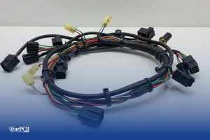
Would your car be able to run without wire harnesses? Not a chance. Wire harnesses connect all the electrical parts together. No harness means no
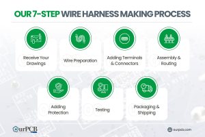
Making wire harnesses isn’t complicated. At OurPCB, we create custom wire harnesses for an expansive range of industries every day. While it’s a complicated process,

Prototype cable assemblies are the very important place in between PCB design ideas and interconnects. OurPCB brings prototype assemblies with PCB solutions to your tables.
PCB thermal management prevents component overheating through strategic heat transfer techniques. Without proper thermal control, electronics are at risk of electronic failures through weakened solder
ContentsKey TakeawaysWhat is a Multilayer-Printed Circuit Board?How do Multilayer PCB Boards Work?Multilayer PCB ApplicationsMultilayer PCB Manufacturing Process: StepsMultilayer PCB Manufacturing MachinesBenefits of Multilayer Circuit BoardsWhat
We use cookies to improve your browsing experience, which may include personal information. By clicking "Agree," you accept our Privacy Policy and cookie use. You can change your cookie settings in your browser anytime.
Agree
 Chat With Us
 Free Quote