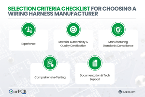
Top 10 Classic Car Wiring Harness Manufacturers | Full Guide
Finding the right wiring harness manufacturer for your vintage ride can be a real headache. Those beautiful old machines need special wiring that looks period-correct

OurPCB provides signal integrity solutions for PCBs requiring exact impedance targets, clean signal paths, and stable reference planes.
We eliminate signal integrity issues like reflections, crosstalk, and distortion by controlling stackup, trace geometry, and dielectric loss at every layer.


As a specialized high speed PCB manufacturer, OurPCB helps engineers and procurement teams resolve PCB signal integrity problems before fabrication by offering detailed design review, material compatibility checks, and stackup validation.
We work with you to identify potential problems in impedance matching, return current routing, and via transitions that could cause signal degradation or failure in timing-sensitive applications.
We return quotes for signal integrity PCB builds in 48 working hours or less, with stackup notes and impedance constraints included. Production lead time ranges from 4 to 25 days, depending on layer count and processing area.
You will receive detailed material and test documentation, and can request a validated test solution for boards that require impedance hold or compliance testing before final assembly.


We review Gerber files, layer stackups, and impedance-critical traces for design features that may compromise PCB signal integrity during manufacturing.
This includes identifying ground plane splits beneath signal layers, mismatched differential signal traces, or impedance discontinuities caused by routing over voids or layer transitions.
Our engineering team flags these conditions before fabrication begins and provides feedback to minimize signal integrity problems such as crosstalk, reflection, and return path disruption.
Reviews are conducted during quoting and pre-production to ensure controlled stackup behavior and consistent electrical performance across all PCB design types.
We manufacture PCBs for systems operating at 10 Gbps and above, where signal quality is affected by edge rate, rise time, and impedance consistency.
Our team reviews stackups and build materials for high-speed interface compatibility and flags risk factors like long stubs, narrow trace widths, or insufficient isolation.
These reviews support better fabrication outcomes for DDR, SerDes, Ethernet, and LVDS channels by helping engineers preserve waveform clarity and reduce jitter or reflections.
OurPCB meets full fabrication standards for automotive, semiconductor, and medical systems, where repeatability and traceability are non-negotiable.
We are certified to ISO 9001, ISO 14001, ISO 13485, IATF 16949, and RoHS, and support IPC-A-610 Class 3 builds when required.
These process controls ensure that plating thickness, pad integrity, and power delivery geometry are manufactured to tight tolerances in production, not just in theory.
All impedance-managed boards undergo TDR, flying probe, and X-ray validation to confirm net continuity, via depth, and alignment accuracy.
These checks detect unexpected signal path discontinuities or reflection points before final shipment.
Paired with test coupons and AOI, this provides early insight into real-world integrity analysis for builds with tight impedance margins or matched differential pairs.
Applications like 5G base stations, ADAS control units, medical imaging systems, and high-speed storage arrays depend on clean signal behavior across every layer and interface. These systems are sensitive to waveform distortion and transmission loss, especially as rise times shorten and trace densities increase.
In these environments, PCB trace geometry, copper distribution, and dielectric spacing all influence waveform accuracy and timing margin. As supply voltage thresholds shrink and signal characteristics become harder to maintain, even small layout variations can cause signal integrity challenges.
OurPCB fabricates boards for these systems using stackups with verified material control and layer consistency to preserve signal transmission performance from driver to receiver.
Telecom equipment must transmit large volumes of data with minimal jitter, delay, or waveform collapse.
High-frequency routing in backplanes and modules often suffers from adjacent signal coupling, where rising edge transitions interfere with nearby traces.
Maintaining integrity in these systems is essential to avoid protocol-level errors, lost packets, or desynchronized channel timing.
In diagnostic systems, analog accuracy and digital response must coexist without cross-interference.
Signal distortion can arise when high-speed lines disrupt analog zones or when grounding and spacing are inconsistent.
These systems often operate with low supply voltage thresholds and minimal margin for waveform deviation.
Timing faults and noise coupling in industrial systems can cause false reads, missed triggers, or control lag.
Trace reflections, mismatched impedance, and EMI exposure are all risks as the signal travels through large boards or remote I/O systems.
Reducing interference across all layers is necessary to keep logic signals discrete and responsive.
Signal integrity is necessary in vehicles where control loops, safety systems, and sensor fusion operate simultaneously.
Over long cable runs or in dense routing zones, signals may degrade due to impedance mismatch or radiated emissions.
Systems such as ADAS, battery management, and infotainment require isolation from power delivery network noise and a reliable waveform shape through each operating cycle.
Waveform integrity is critical in high-precision instruments and machine-to-machine control loops. Even minor distortion can affect measurement resolution or sample validity. These environments depend on strong isolation, clean routing, and uninterrupted signal edges to maintain signal performance across all data acquisition paths.
test
Maintaining signal integrity on PCB designs requires precise control of impedance, routing, and material behavior across every layer and interconnect. OurPCB fabricates circuit boards that reduce distortion and reflections through engineered stackups, dielectric consistency, and well-defined return paths.
We manufacture PCB stackups to maintain signal integrity through consistent impedance across transmission lines, differential pairs, and return paths. We maintain symmetrical stackup structures and low-Dk laminates using impedance within ±5Ω for lines under 50 Ω and ±10% for those above 50 Ω, as defined in IPC-TM-650 tests.
Each signal layer is paired with a continuous ground or power plane to control signal return and reduce EMI, while transitions are modeled for characteristic impedance consistency.
Our builds support stripline and microstrip routing with layer counts up to 40, including 18-layer HDI interconnects and hybrid stackups using Rogers RO4000, Panasonic R-5785(M7), or Taconic RF-35 for high-speed signal preservation.
We use low-loss dielectric systems to reduce signal degradation and preserve waveform integrity across high-frequency traces and controlled impedance lines. Your material options include Rogers RO3000/RO4000, Panasonic R-5785(M7), and Arlon 25 N.
These substrates limit rise-time distortion, phase shift, and transmission loss, particularly in designs where signal speeds increase and precision timing is required. These laminates maintain consistent PCB signal integrity across every interconnect layer when combined with impedance-managed stackups and tightly matched trace geometries.
OurPCB fabricates controlled impedance PCBs with trace widths and spacings tailored to copper weight, signal layer type, and impedance class.
Outer layer geometries follow similar controls, with 2.0/2.0 mil achievable at 25 μm finished copper, scaling to 8/8 mil at 210 μm. These constraints are enforced to prevent impedance discontinuity, minimize signal reflections, and reduce crosstalk between adjacent traces.
OurPCB manufactures via structures with controlled geometry and plating to reduce parasitic inductance and maintain signal fidelity at layer transitions. Mechanical drill sizes reach down to 0.08 mm, and we handle blind, buried, stacked, and via-in-pad types across multilayer and HDI boards.
For high-speed interconnects, laser-drilled microvias as small as 3 mil are resin-filled and plated to suppress impedance discontinuities. Our process supports via aspect ratios up to 40:1, with X-ray alignment and plating verification. Engineering teams provide via structure review to help limit jitter, reflections, and coupling on sensitive signal paths.
Clean signal return is a requirement for stable impedance and reduced electromagnetic interference. OurPCB manufactures PCBs with symmetrical stackups where each signal layer is paired with a continuous reference plane, preventing disruption of return current.
To minimize loop area, we maintain reference plane continuity across vias and eliminate copper splits beneath signal transitions. Where required, we apply edge plating and metal-filled shielding vias around perimeter zones or differential lines to reduce coupling and contain fringe fields.
Controlled depth slots and stepped isolation channels are machined with tolerances of ±0.2 mm to direct current return flow away from high-speed traces. Return path integrity is reviewed during pre-production, and design violations such as split-plane crossings or narrow isolation gaps are flagged for correction before fabrication.
OurPCB performs in-process and final signal integrity analysis and impedance verification using standards-based test protocols to confirm signal integrity on manufactured boards. Impedance control is validated to ±5Ω (<50 Ω) and ±10% (≥50 Ω) using simulation methods defined in IPC-TM-650 and verified through both test coupons and TDR measurements.
Boards with differential pairs, high-speed nets, or stripline structures are reviewed for uniform impedance across layer transitions and validated post-fabrication using flying probe, X-ray target drilling, and electrical test. When required, resonance cavities, controlled-depth features, and blind via structures are evaluated for discontinuities affecting return loss and jitter.
Signal degradation risks are flagged by our process engineers during build review and measured using structured net models where relevant. These steps help reduce variation across the production panel and improve signal quality in timing-critical applications.
Maintaining signal integrity on PCB designs requires precise control of impedance, routing, and material behavior across every layer and interconnect. OurPCB fabricates circuit boards that reduce distortion and reflections through engineered stackups, dielectric consistency, and well-defined return paths.
We manufacture PCB stackups to maintain signal integrity through consistent impedance across transmission lines, differential pairs, and return paths. We maintain symmetrical stackup structures and low-Dk laminates using impedance within ±5Ω for lines under 50 Ω and ±10% for those above 50 Ω, as defined in IPC-TM-650 tests.
Each signal layer is paired with a continuous ground or power plane to control signal return and reduce EMI, while transitions are modeled for characteristic impedance consistency.
Our builds support stripline and microstrip routing with layer counts up to 40, including 18-layer HDI interconnects and hybrid stackups using Rogers RO4000, Panasonic R-5785(M7), or Taconic RF-35 for high-speed signal preservation.
We use low-loss dielectric systems to reduce signal degradation and preserve waveform integrity across high-frequency traces and controlled impedance lines. Your material options include Rogers RO3000/RO4000, Panasonic R-5785(M7), and Arlon 25 N.
These substrates limit rise-time distortion, phase shift, and transmission loss, particularly in designs where signal speeds increase and precision timing is required. These laminates maintain consistent PCB signal integrity across every interconnect layer when combined with impedance-managed stackups and tightly matched trace geometries.
OurPCB fabricates controlled impedance PCBs with trace widths and spacings tailored to copper weight, signal layer type, and impedance class.
Outer layer geometries follow similar controls, with 2.0/2.0 mil achievable at 25 μm finished copper, scaling to 12/12 mil at 210 μm. These constraints are enforced to prevent impedance discontinuity, minimize signal reflections, and reduce crosstalk between adjacent traces.
OurPCB manufactures via structures with controlled geometry and plating to reduce parasitic inductance and maintain signal fidelity at layer transitions. Mechanical drill sizes reach down to 0.1 mm, and we handle blind, buried, stacked, and via-in-pad types across multilayer and HDI boards.
For high-speed interconnects, laser-drilled microvias as small as 3 mil are resin-filled and plated to suppress impedance discontinuities. Our process supports via aspect ratios up to 25:1, with X-ray alignment and plating verification. Engineering teams provide via structure review to help limit jitter, reflections, and coupling on sensitive signal paths.
Clean signal return is a requirement for stable impedance and reduced electromagnetic interference. OurPCB manufactures PCBs with symmetrical stackups where each signal layer is paired with a continuous reference plane, preventing disruption of return current.
To minimize loop area, we maintain reference plane continuity across vias and eliminate copper splits beneath signal transitions. Where required, we apply edge plating and metal-filled shielding vias around perimeter zones or differential lines to reduce coupling and contain fringe fields.
Controlled depth slots and stepped isolation channels are machined with tolerances of ±0.2 mm to direct current return flow away from high-speed traces. Return path integrity is reviewed during pre-production, and design violations such as split-plane crossings or narrow isolation gaps are flagged for correction before fabrication.
OurPCB performs in-process and final signal integrity analysis and impedance verification using standards-based test protocols to confirm signal integrity on manufactured boards. Impedance control is validated to ±5Ω (<50 Ω) and ±10% (≥50 Ω) using simulation methods defined in IPC-TM-650 and verified through both test coupons and TDR measurements.
Boards with differential pairs, high-speed nets, or stripline structures are reviewed for uniform impedance across layer transitions and validated post-fabrication using flying probe, X-ray target drilling, and electrical test. When required, resonance cavities, controlled-depth features, and blind via structures are evaluated for discontinuities affecting return loss and jitter.
Signal degradation risks are flagged by our process engineers during build review and measured using structured net models where relevant. These steps help reduce variation across the production panel and improve signal quality in timing-critical applications.
Mon-Fri: 24 hours,
Sat: 9am-6pm, GMT+8
Reach us at
[email protected]
24 hours online
+86-199-30589219
Mon-Fri: 24 hours,
Sat: 9am-6pm, GMT+8
Signal integrity in PCB systems refers to the ability of a signal to retain its original shape, timing, and amplitude as it moves across traces and layers. Poor routing, inconsistent materials, or layer transitions can cause reflections, timing skew, or distortion that alters the waveform and introduces logic errors.
Engineers use PCB design and analysis techniques to evaluate these risks and improve signal clarity before final layout and fabrication.
Vias change the electrical path of a signal by introducing parasitic inductance, capacitance, and physical discontinuities. These effects can distort waveforms as they pass between layers, especially when edge rates are fast or when the via length is not managed correctly.
Design simulation tools help visualize how signal edges degrade around vias and guide decisions about stub removal, backdrilling, or via placement to preserve timing accuracy.
Signal reflections occur when a waveform encounters a sudden change in impedance along its path, such as at connector interfaces, via transitions, or trace width shifts.
These mismatches cause part of the transmitted signal to bounce back toward the source, which can interfere with the next edge or corrupt timing. Careful control of the PCB trace geometry and consistent layer transitions help minimize these effects in the layout.
Stack-up design improves signal quality by controlling electromagnetic field behavior across signal layers and adjacent planes. Proper placement of ground and power planes limits the inductive loop area and keeps return current paths tightly coupled to the signal layer, which reduces noise and reflections.
A well-structured stackup balances dielectric thickness and material properties to maintain uniform propagation delay, isolate analog and digital zones, and prevent unintended coupling between signal nets.
OurPCB verifies signal integrity using Time Domain Reflectometry (TDR) on dedicated test coupons to confirm impedance within specified tolerances, such as ±5Ω or ±10%. AOI, X-ray, and flying probe testing are performed to detect structural issues like drill misalignment, voids, or open connections that may impact waveform stability.
These tests are part of the fabrication process and help validate that signal-carrying nets are manufactured to electrical and geometric standards.
Materials like Rogers RO3000, RO4000, Taconic RF-35, Panasonic R-5785(M7), Arlon 25 N, and PTFE-based ceramic blends are used for high-speed signal transmission because they offer low dielectric constant (Dk) and low dissipation factor (Df).
These electrical properties help minimize waveform loss, maintain signal velocity, and preserve timing at multi-GHz frequencies. Their stable performance across temperature and frequency ranges makes them suitable for impedance-controlled designs where edge shape and phase alignment must be preserved.
Impedance control in PCB design refers to maintaining a consistent characteristic impedance along signal traces to prevent reflections and signal distortion.
This is achieved by carefully managing trace width, dielectric height, and material properties so the signal sees a uniform electrical environment as it travels. Controlled impedance is especially important for transmission lines carrying high-speed or timing-sensitive signals, where even small discontinuities can cause data errors.
To reduce crosstalk and electromagnetic interference (EMI) in a PCB, signals must be physically and electrically isolated using controlled spacing, layer stacking, and reference plane continuity.
Crosstalk is minimized by increasing the distance between adjacent signal traces and avoiding parallel routing across long distances. EMI is reduced by routing signal return paths over continuous ground planes and isolating noisy nets from sensitive zones through proper PCB layout and layer planning.
OurPCB delivers PCB signal integrity solutions with tightly controlled stackups, trace geometry, and verified impedance to support performance in SI-sensitive designs. Request a quote today to review your stackup and fabrication plan with our engineering team.
Finding the right wiring harness manufacturer for your vintage ride can be a real headache. Those beautiful old machines need special wiring that looks period-correct
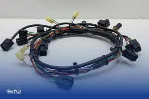
Would your car be able to run without wire harnesses? Not a chance. Wire harnesses connect all the electrical parts together. No harness means no
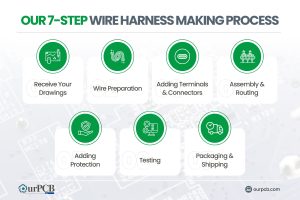
Making wire harnesses isn’t complicated. At OurPCB, we create custom wire harnesses for an expansive range of industries every day. While it’s a complicated process,

Prototype cable assemblies are the very important place in between PCB design ideas and interconnects. OurPCB brings prototype assemblies with PCB solutions to your tables.
PCB thermal management prevents component overheating through strategic heat transfer techniques. Without proper thermal control, electronics are at risk of electronic failures through weakened solder
ContentsKey TakeawaysWhat is a Multilayer-Printed Circuit Board?How do Multilayer PCB Boards Work?Multilayer PCB ApplicationsMultilayer PCB Manufacturing Process: StepsMultilayer PCB Manufacturing MachinesBenefits of Multilayer Circuit BoardsWhat
We use cookies to improve your browsing experience, which may include personal information. By clicking "Agree," you accept our Privacy Policy and cookie use. You can change your cookie settings in your browser anytime.
Agree
 Chat With Us
 Free Quote