

IPC/WHMA-A-620: The Complete Wire Harness Audit Guide for Chinese Factories
IPC/WHMA-A-620 is the main inspection and acceptance standard for cable and wire harness assemblies. If you source wire harnesses from China, put this standard at
 5 Star Rating on
 As a high speed PCB manufacturer, OurPCB fabricates multilayer printed circuit boards with controlled impedance, low-loss substrates, and high-frequency performance.
We support up to 64-layer stackups using materials such as Rogers, PTFE, and Megtron-class laminates for reliable signal transmission.


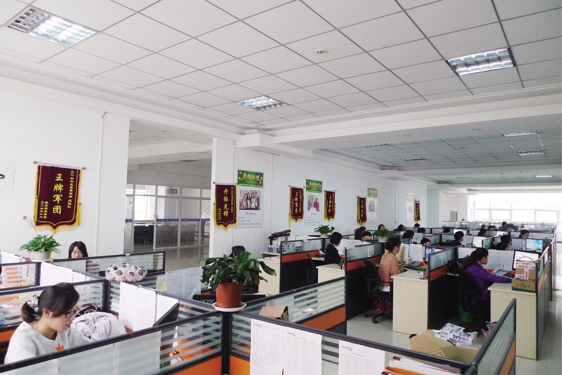
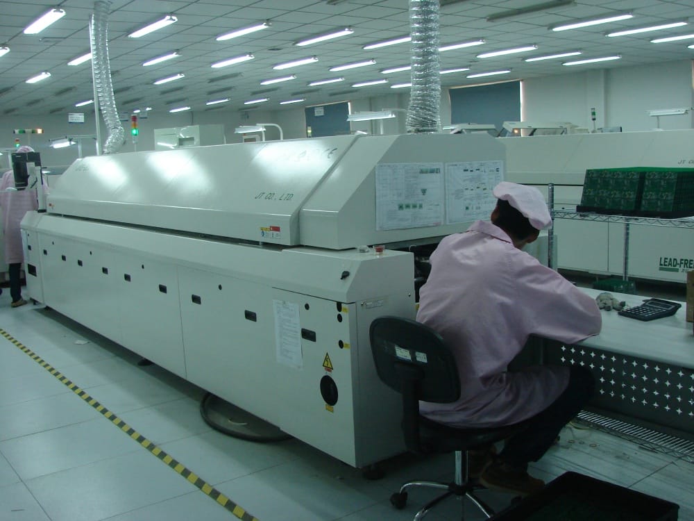
OurPCB operates two high-capacity factories in Shijiazhuang and Shenzhen, with over 15,000 square meters of combined production space.
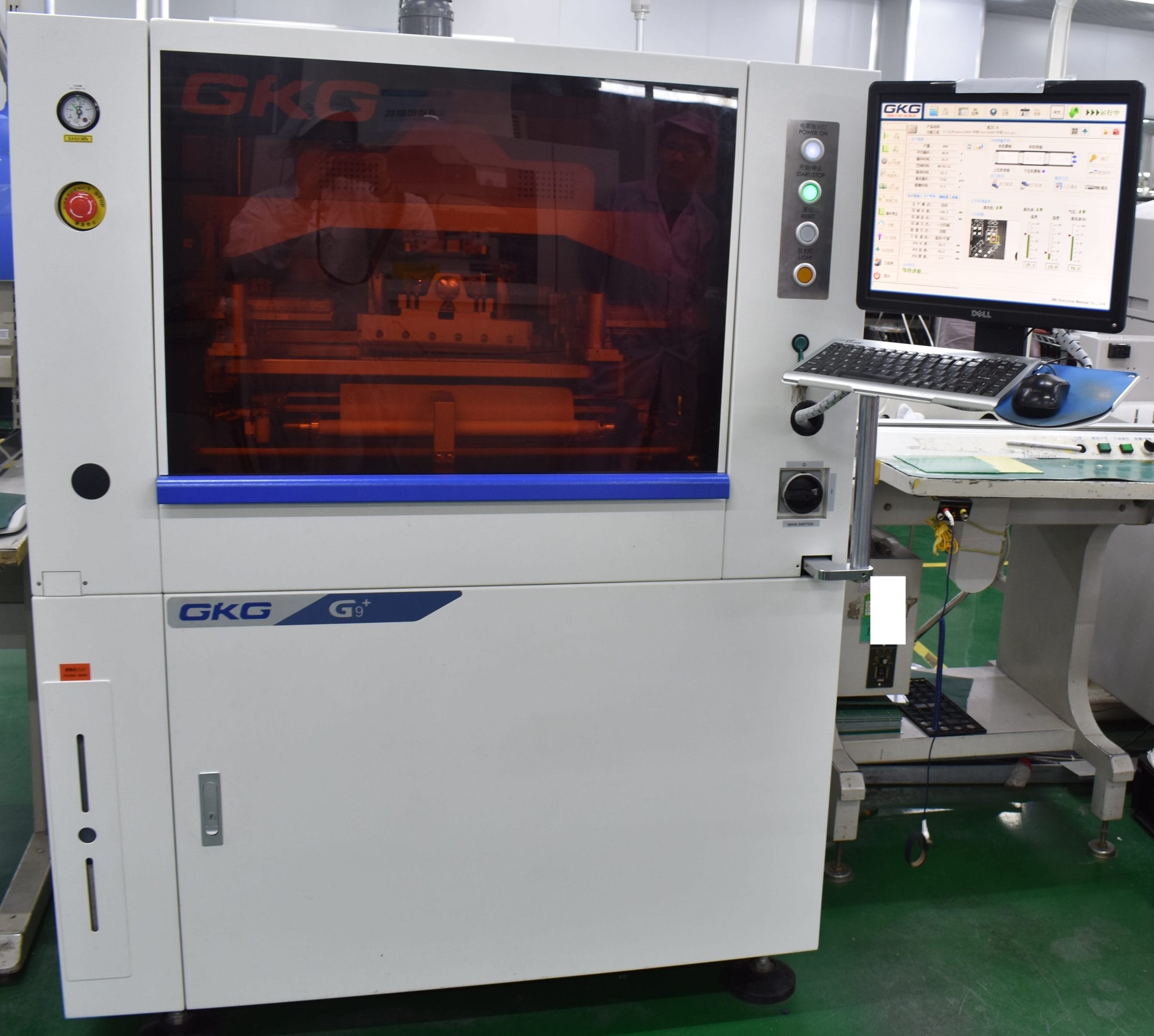
We process high-speed multilayer PCBs on dedicated lines equipped with LDI exposure units, PTH copper sinking lines, and AOI stations optimized for fine-line trace analysis.

All impedance-controlled PCBs undergo staged inspection using optical AOI (automated optical inspection), flying probe continuity test, and 4-wire low resistance measurement systems.
Resistance testing accuracy reaches ±0.01 mΩ, essential for validating copper integrity in power-ground planes and differential trace pairs.
This multi-method inspection minimizes propagation delay mismatches and signal distortion in high-speed designs.

Our engineering and process teams evaluate every high-speed order before production release.
Stackup validation includes dielectric constant modeling, copper roughness correction, and impedance calculations per IPC-2141.
DFM review includes trace width/spacing, return path alignment, via clearance, and tolerance stacking for designs using PTFE, hydrocarbon, or ceramic-filled systems.

To ensure adhesion between inner layer cores and prepreg during lamination, all copper surfaces undergo brown oxide treatment and wet chemical cleaning.
This process creates a micro-etched copper oxide surface for optimal epoxy resin anchoring.
Controlled oxide thickness and pre-bond surface conditioning prevent delamination in high-aspect-ratio multilayer stackups during press cycles.

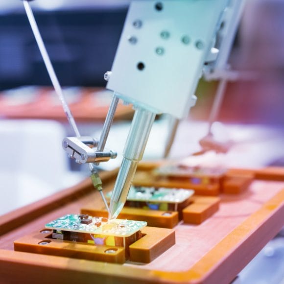
For high-speed PCB assemblies involving complex ICs, high-speed interfaces, or tight-pitch components, OurPCB performs X-ray inspection, optical joint analysis, and continuity testing using programmable digital power supplies.
Signal-critical paths such as DDR, PCIe, and USB interfaces are verified for routing integrity and solder joint performance under post-reflow conditions.
These inspection steps ensure clean impedance transitions, matched routing paths, and electrical compliance across the complete assembled board.

As a high speed PCB manufacturer, we manage process yield not only at the final test but also across drilling, copper plating, lamination, soldermask, surface finish, and routing.
Each stage includes AOI or metrology checkpoints using microscopes, resistance testers, or X-ray inspection.
This step-by-step product quality check prevents compounding defects in high-speed PCBs, where a single misregistration or plating void can result in signal reflection or impedance failure.
![]()
OurPCB operates two high-capacity factories in Shijiazhuang and Shenzhen, with over 15,000 square meters of combined production space.
We deliver comprehensive signal integrity PCB solutions by processing high-speed multilayer PCBs on dedicated lines equipped with LDI exposure units, PTH copper sinking lines, and AOI stations optimized for fine-line trace analysis.Retry
![]()
All impedance-controlled PCBs undergo staged inspection using optical AOI (automated optical inspection), flying probe continuity test, and 4-wire low resistance measurement systems.
Resistance testing accuracy reaches ±0.01 mΩ, essential for validating copper integrity in power-ground planes and differential trace pairs.
This multi-method inspection minimizes propagation delay mismatches and signal distortion in high-speed designs.
![]()
Our engineering and process teams evaluate every high-speed order before production release.
Stackup validation includes dielectric constant modeling, copper roughness correction, and impedance calculations per IPC-2141.
DFM review includes trace width/spacing, return path alignment, via clearance, and tolerance stacking for designs using PTFE, hydrocarbon, or ceramic-filled systems.
![]()
To ensure adhesion between inner layer cores and prepreg during lamination, all copper surfaces undergo brown oxide treatment and wet chemical cleaning.
This process creates a micro-etched copper oxide surface for optimal epoxy resin anchoring.
Controlled oxide thickness and pre-bond surface conditioning prevent delamination in high-aspect-ratio multilayer stackups during press cycles.
![]()
For high-speed PCB assemblies involving complex ICs, high-speed interfaces, or tight-pitch components, OurPCB performs X-ray inspection, optical joint analysis, and continuity testing using programmable digital power supplies.
Signal-critical paths such as DDR, PCIe, and USB interfaces are verified for routing integrity and solder joint performance under post-reflow conditions.
These inspection steps ensure clean impedance transitions, matched routing paths, and electrical compliance across the complete assembled board.
![]()
As a high speed PCB manufacturer, we manage process yield not only at the final test but also across drilling, copper plating, lamination, soldermask, surface finish, and routing.
Each stage includes AOI or metrology checkpoints using microscopes, resistance testers, or X-ray inspection.
This step-by-step product quality check prevents compounding defects in high-speed PCBs, where a single misregistration or plating void can result in signal reflection or impedance failure.
![]()
Rogers / Arlon, Panasonic, Isola, TUC (Taiwan Union Technology), EMC (Elite Material Co.), ITEQ, VENTEC, Shengyi Technology, Taconic, Nelco, Taizhou Wangling, ZhongYing Technology, FSD, Gaussbell, Ruilong, Guoneng, Yinghua, Mitsubishi Gas Chemical, Doosan, Nan Ya Plastics

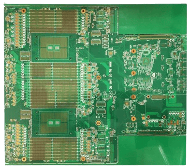
We fabricate high-speed PCBs for ADAS, radar modules, and infotainment systems that require stable high-speed signal performance under extreme conditions.
Each multilayer PCB includes matched trace lengths and controlled impedance for protocols like PCIe and LVDS, maintaining accurate data transfer rates across shielded routing layers.

Impedance-controlled builds for 10GbE, 25GbE, and QSFP network systems need a high speed PCB manufacturer.
These circuit boards are designed with differential pair tuning and dielectric stackups that minimize loss and signal skew, enabling consistent high-speed data throughput in optical and copper-based infrastructure.

Our high-frequency PCBs enable real-time diagnostics, telemetry, and high-resolution imaging in compact medical platforms.
These designs often combine PTFE or ceramic-filled cores with HDI routing to maintain signal quality.
We focus on fabricating high-speed interconnects that meet the strict accuracy demands of medical systems.

We manufacture advanced circuits for industrial automation, edge controllers, and FPGA-based systems that require consistent timing and low EMI across complex stackups.
High-speed boards in this space need careful modeling of dielectric constant and copper profile to maintain signal integrity in harsh environments.

We fabricate high-speed PCBs for USB 3.2, DDR5, and Thunderbolt-enabled devices that require consistent impedance and clean return paths.
Each board has HDI routing, copper thickness control, and matched trace lengths to maintain signal timing and reduce EMI.
These stackups are engineered to meet specific high-speed PCB needs in consumer products operating at gigabit-level speeds.

We manufacture high-speed PCBs for aerospace telemetry modules, radar systems, and RF communication platforms in satellite and defense applications.
These systems require precise impedance control, stable dielectric properties, and long-term reliability under extreme thermal and vibration conditions.
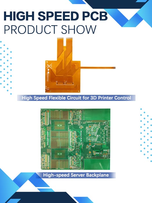
Our production includes rigid, rigid-flex, and HDI constructions across multiple types of PCBs, each fabricated to maintain high-speed signal integrity across extended transmission paths.

![]()
We fabricate high-speed PCBs for ADAS, radar modules, and infotainment systems that require stable high-speed signal performance under extreme conditions.
Each multilayer PCB includes matched trace lengths and controlled impedance for protocols like PCIe and LVDS, maintaining accurate data transfer rates across shielded routing layers.
![]()
Impedance-controlled builds for 10GbE, 25GbE, and QSFP network systems need a high speed PCB manufacturer.
These circuit boards are designed with differential pair tuning and dielectric stackups that minimize loss and signal skew, enabling consistent high-speed data throughput in optical and copper-based infrastructure.
![]()
Our high-frequency PCBs enable real-time diagnostics, telemetry, and high-resolution imaging in compact medical platforms.
These designs often combine PTFE or ceramic-filled cores with HDI routing to maintain signal quality.
We focus on fabricating high-speed interconnects that meet the strict accuracy demands of medical systems.
![]()
We manufacture advanced circuits for industrial automation, edge controllers, and FPGA-based systems that require consistent timing and low EMI across complex stackups.
High-speed boards in this space need careful modeling of dielectric constant and copper profile to maintain signal integrity in harsh environments.
![]()
We fabricate high-speed PCBs for USB 3.2, DDR5, and Thunderbolt-enabled devices that require consistent impedance and clean return paths.
Each board has HDI routing, copper thickness control, and matched trace lengths to maintain signal timing and reduce EMI.
These stackups are engineered to meet specific high-speed PCB needs in consumer products operating at gigabit-level speeds.
![]()
We manufacture high-speed PCBs for aerospace telemetry modules, radar systems, and RF communication platforms in satellite and defense applications.
These systems require precise impedance control, stable dielectric properties, and long-term reliability under extreme thermal and vibration conditions.
Our production includes rigid, rigid-flex, and HDI constructions across multiple types of PCBs, each fabricated to maintain high-speed signal integrity across extended transmission paths.
You need a high speed PCB manufacturer when a standard PCB isn’t sufficient for your needs. High-speed PCBs are necessary when signal behavior is affected by transmission line effects, which occur when the trace length exceeds one-tenth to one-twelfth of the signal’s wavelength.
For example, a 1 GHz signal has a wavelength of approximately 30 cm on FR4, meaning any trace longer than 2.5 to 3 cm must be treated as a transmission line. A high-speed layout is also required when the trace delay exceeds 20% of the signal’s rise time, a common issue in fast-switching digital systems where rise times are under 1 ns.
If your design includes interfaces like DDR4/DDR5, PCIe Gen 4/5, USB 3.2, SATA, or MIPI, it qualifies as high-speed. Other indicators include differential pairs, matched trace routing, layer-specific signal referencing, or the need to simulate crosstalk, reflection, and skew across interconnects. These conditions require controlled routing, accurate dielectric modeling, and trace geometry tailored to maintain timing integrity across layers.
We source and process high-speed laminates, including Rogers RO4000 and RO3000, Arlon AD and TC series, Panasonic R-5775(M6)/R-5785(M7), and Taconic TLX and RF-35, offering dielectric constants from 2.2 to 3.5 and dissipation factors as low as 0.0018.
Our experienced team chooses material configurations based on design frequency, layer count, and stackup structure using bonding films like RO4400 or 25FR. For hybrid multilayers, we enable localized bonding between PTFE and FR4 using epoxy or PPO/PPE blends.
OurPCB builds multilayer PCBs up to 40 layers, although we’ll need to review stackups exceeding 36 layers. All layer constructions use symmetrical copper weight distribution, alternating power and ground planes, and precisely specified dielectric thicknesses as low as 3 mils.
Materials include epoxy, hydrocarbon, and ceramic-filled PTFE laminates, depending on frequency and impedance targets. Finished board thickness ranges from 0.3 mm to 10 mm, constrained by layer count and copper weight. Every stackup is designed for impedance control between 45 Ω and 90 Ω and evaluated for interplane isolation, return path integrity, and manufacturability.
Our technicians fabricate controlled impedance traces with width and spacing tolerances based on copper weight and layer position. Outer layers with finished copper thickness of 35–53 μm allow 3.5/3.5 mil line/space; inner layers with 12 μm copper enable 2.5/2.5 mil resolution. Differential pair and microstrip configurations are matched to 50 Ω ±5 Ω or custom values per IPC-2141 calculations.
Return paths are enforced through uninterrupted ground planes, and all impedance-critical traces undergo trace length tuning, skew adjustment, and spacing verification during layout review. Impedance coupon analysis and TDR validation are included in production to confirm signal performance.
OurPCB manufactures high-speed HDI PCBs with laser-drilled microvias down to 3 mils in diameter and via-in-pad structures with copper filling and resin plugging. The maximum HDI stackup configuration is 8+2+8 with up to 8 sequential laminations per core.
Blind and buried vias are available in single, double, and triple-press configurations with symmetrical structure control, and all builds are reviewed when using stacked or cross-blind vias. Press-fit, back-drilled, and copper-filled options are available for signal isolation, thermal relief, or EMI mitigation.
OurPCB assembles high-speed PCBs with a placement accuracy of ±30 microns using automated SMT lines equipped for 01005 components. All assemblies conform to IPC-A-610H Class 2 or 3 workmanship, with trace and pad dimensional fidelity maintained within ±75 microns after reflow.
As a high speed PCB manufacturer, we perform DFM and signal integrity validation using HyperLynx, Altium Designer, and IPC-2141 modeling tools. Impedance traces are simulated using stackup-specific dielectric constants (Dk) from 2.2 to 3.9 and dissipation factors (Df) as low as 0.0018, based on materials like Rogers RO4000, Panasonic R-5775(M6), and Taconic TLX.
Simulations include copper surface roughness correction and skin effect modeling for high-speed transmission lines.
OurPCB provides high-speed PCB prototypes in as little as 4 working days for 2-layer builds under 1m², and up to 14 working days for 12-layer boards under 3m². All impedance-controlled designs include test coupons and undergo AOI, X-ray, and electrical testing per IPC-6012E and IPC-TM-650.
Impedance is verified using TDR analysis with tolerance bands held to ±5Ω for single-ended and differential traces. Designs exceeding 36 layers, greater than 420 μm copper thickness, or involving hybrid dielectric systems require engineering review before PCB manufacturing.
We source and process high-speed laminates, including Rogers RO4000 and RO3000, Arlon AD and TC series, Panasonic R-5775(M6)/R-5785(M7), and Taconic TLX and RF-35, offering dielectric constants from 2.2 to 3.5 and dissipation factors as low as 0.0018.
Our experienced team chooses material configurations based on design frequency, layer count, and stackup structure using bonding films like RO4400 or 25FR. For hybrid multilayers, we enable localized bonding between PTFE and FR4 using epoxy or PPO/PPE blends.
OurPCB builds multilayer PCBs up to 64 layers, although we’ll need to review stackups exceeding 36 layers. All layer constructions use symmetrical copper weight distribution, alternating power and ground planes, and precisely specified dielectric thicknesses as low as 3 mils.
Materials include epoxy, hydrocarbon, and ceramic-filled PTFE laminates, depending on frequency and impedance targets. Finished board thickness ranges from 0.1 mm to 12 mm, constrained by layer count and copper weight. Every stackup is designed for impedance control between 45 Ω and 90 Ω and evaluated for interplane isolation, return path integrity, and manufacturability.
Our technicians fabricate controlled impedance traces with width and spacing tolerances based on copper weight and layer position. Outer layers with finished copper thickness of 25 μm allow 2/2 mil line/space; inner layers with 12 μm copper enable 1.8/1.8 mil resolution. Differential pair and microstrip configurations are matched to 50 Ω ±5 Ω or custom values per IPC-2141 calculations.
Return paths are enforced through uninterrupted ground planes, and all impedance-critical traces undergo trace length tuning, skew adjustment, and spacing verification during layout review. Impedance coupon analysis and TDR validation are included in production to confirm signal performance.
OurPCB manufactures high-speed HDI PCBs with laser-drilled microvias down to 3 mils in diameter and via-in-pad structures with copper filling and resin plugging. The maximum HDI stackup configuration is 8+n+8 with up to 8 sequential laminations per core.
Blind and buried vias are available in single, double, and triple-press configurations with symmetrical structure control, and all builds are reviewed when using stacked or cross-blind vias. Press-fit, back-drilled, and copper-filled options are available for signal isolation, thermal relief, or EMI mitigation.
OurPCB assembles high-speed PCBs with a placement accuracy of ±30 microns using automated SMT lines equipped for 01005 components. All assemblies conform to IPC-A-610H Class 2 or 3 workmanship, with trace and pad dimensional fidelity maintained within ±75 microns after reflow.
As a high speed PCB manufacturer, we perform DFM and signal integrity validation using HyperLynx, Altium Designer, and IPC-2141 modeling tools. Impedance traces are simulated using stackup-specific dielectric constants (Dk) from 2.2 to 3.9 and dissipation factors (Df) as low as 0.0018, based on materials like Rogers RO4000, Panasonic R-5775(M6), and Taconic TLX.
Simulations include copper surface roughness correction and skin effect modeling for high-speed transmission lines.
OurPCB provides high-speed PCB prototypes in as little as 4 working days for 2-layer builds under 1m², and up to 14 working days for 12-layer boards under 3m². All impedance-controlled designs include test coupons and undergo AOI, X-ray, and electrical testing per IPC-6012E and IPC-TM-650.
Impedance is verified using TDR analysis with tolerance bands held to ±5Ω for single-ended and differential traces. Designs exceeding 36 layers, greater than 525 μm copper thickness, or involving hybrid dielectric systems require engineering review before PCB manufacturing.

OurPCB operates two high-capacity factories in Shijiazhuang and Shenzhen, with over 10,000 square meters of combined production space.
We process high-speed multilayer PCBs on dedicated lines equipped with LDI exposure units, PTH copper sinking lines, and AOI stations optimized for fine-line trace analysis.

All impedance-controlled PCBs undergo staged inspection using optical AOI (automated optical inspection), flying probe continuity test, and 4-wire low resistance measurement systems.
Resistance testing accuracy reaches ±0.01 mΩ, essential for validating copper integrity in power-ground planes and differential trace pairs.
This multi-method inspection minimizes propagation delay mismatches and signal distortion in high-speed designs.

Our engineering and process teams evaluate every high-speed order before production release.
Stackup validation includes dielectric constant modeling, copper roughness correction, and impedance calculations per IPC-2141.
DFM review includes trace width/spacing, return path alignment, via clearance, and tolerance stacking for designs using PTFE, hydrocarbon, or ceramic-filled systems.

To ensure adhesion between inner layer cores and prepreg during lamination, all copper surfaces undergo brown oxide treatment and wet chemical cleaning.
This process creates a micro-etched copper oxide surface for optimal epoxy resin anchoring.
Controlled oxide thickness and pre-bond surface conditioning prevent delamination in high-aspect-ratio multilayer stackups during press cycles.

For high-speed PCB assemblies involving complex ICs, high-speed interfaces, or tight-pitch components, OurPCB performs X-ray inspection, optical joint analysis, and continuity testing using programmable digital power supplies.
Signal-critical paths such as DDR, PCIe, and USB interfaces are verified for routing integrity and solder joint performance under post-reflow conditions.
These inspection steps ensure clean impedance transitions, matched routing paths, and electrical compliance across the complete assembled board.

As a high speed PCB manufacturer, we manage process yield not only at the final test but also across drilling, copper plating, lamination, soldermask, surface finish, and routing.
Each stage includes AOI or metrology checkpoints using microscopes, resistance testers, or X-ray inspection.
This step-by-step product quality check prevents compounding defects in high-speed PCBs, where a single misregistration or plating void can result in signal reflection or impedance failure.

We fabricate high-speed PCBs for ADAS, radar modules, and infotainment systems that require stable high-speed signal performance under extreme conditions.
Each multilayer PCB includes matched trace lengths and controlled impedance for protocols like PCIe and LVDS, maintaining accurate data transfer rates across shielded routing layers.

Impedance-controlled builds for 10GbE, 25GbE, and QSFP network systems need a high speed PCB manufacturer.
These circuit boards are designed with differential pair tuning and dielectric stackups that minimize loss and signal skew, enabling consistent high-speed data throughput in optical and copper-based infrastructure.

Our high-frequency PCBs enable real-time diagnostics, telemetry, and high-resolution imaging in compact medical platforms.
These designs often combine PTFE or ceramic-filled cores with HDI routing to maintain signal quality.
We focus on fabricating high-speed interconnects that meet the strict accuracy demands of medical systems.

We manufacture advanced circuits for industrial automation, edge controllers, and FPGA-based systems that require consistent timing and low EMI across complex stackups.
High-speed boards in this space need careful modeling of dielectric constant and copper profile to maintain signal integrity in harsh environments.

We fabricate high-speed PCBs for USB 3.2, DDR5, and Thunderbolt-enabled devices that require consistent impedance and clean return paths.
Each board has HDI routing, copper thickness control, and matched trace lengths to maintain signal timing and reduce EMI.
These stackups are engineered to meet specific high-speed PCB needs in consumer products operating at gigabit-level speeds.

We manufacture high-speed PCBs for aerospace telemetry modules, radar systems, and RF communication platforms in satellite and defense applications.
These systems require precise impedance control, stable dielectric properties, and long-term reliability under extreme thermal and vibration conditions.
Our production includes rigid, rigid-flex, and HDI constructions across multiple types of PCBs, each fabricated to maintain high-speed signal integrity across extended transmission paths.
You need a high speed PCB manufacturer when a standard PCB isn’t sufficient for your needs. High-speed PCBs are necessary when signal behavior is affected by transmission line effects, which occur when the trace length exceeds one-tenth to one-twelfth of the signal’s wavelength.
For example, a 1 GHz signal has a wavelength of approximately 30 cm on FR4, meaning any trace longer than 2.5 to 3 cm must be treated as a transmission line. A high-speed layout is also required when the trace delay exceeds 20% of the signal’s rise time, a common issue in fast-switching digital systems where rise times are under 1 ns.
If your design includes interfaces like DDR4/DDR5, PCIe Gen 4/5, USB 3.2, SATA, or MIPI, it qualifies as high-speed. Other indicators include differential pairs, matched trace routing, layer-specific signal referencing, or the need to simulate crosstalk, reflection, and skew across interconnects. These conditions require controlled routing, accurate dielectric modeling, and trace geometry tailored to maintain timing integrity across layers.
Mon-Fri: 24 hours,
Sat: 9am-6pm, GMT+8
Reach us at
sales@ourpcb.net
24 hours online
+86-199-30589219
Mon-Fri: 24 hours
Sat: 9am-6pm, GMT+8
A high-speed PCB is a circuit board where signal delay, edge rate, and trace geometry interact in ways that require controlled design rules and fabrication processes. This occurs when the signal’s rise time is short enough that the interconnect behaves like a transmission line, most often when trace delay exceeds 20% of the rise time or the routing exceeds λ/12.
Interfaces like PCIe Gen4, DDR5, and USB 3.2 fall into this category. These boards require matched trace lengths, reference plane continuity, and carefully constructed stackup structures across multilayer PCB builds to minimize signal distortion and skew.
We fabricate high-speed PCBs using low-loss materials, including PTFE-based systems such as Rogers RO3000, Panasonic R-5775(M6), and Arlon 25N, with dielectric constants between 2.2 and 3.9.
These materials support frequencies up to 25 GHz and maintain signal fidelity by reducing insertion loss and dispersion. For sub-2 GHz designs, we use high-Tg FR4 systems like TU-883, balancing cost with adequate performance.
All laminates are selected to match target layer count, copper weight, and routing density, and are documented in our controlled material list for high-speed builds.
Signal behavior is controlled by defining a precise stackup, maintaining trace spacing tolerances, and simulating rise-time impacts using IPC-2141. Our engineering team validates layer order, material Dk/Df, and copper roughness before fabrication.
The inner layer routing is matched to ±10 mil for differential pairs, and all critical paths are aligned with uninterrupted reference planes. Each board includes impedance coupons and undergoes TDR testing to confirm signal integrity across transitions.
These steps are implemented in prototype PCB orders and production to preserve waveform accuracy and reduce reflection and skew.
Yes, we manufacture high-speed PCBs with stacked HDI architectures up to 8+n+8 layers using blind, buried, and laser-drilled microvias down to 3 mils. Resin-filled via-in-pad is applied for fine-pitch components such as BGA and SiP.
Laser hole depth control is maintained to ±20 μm, and via cap flattening ensures clean surface mount compatibility. These features are standard in rigid-flex PCB designs and advanced interconnect modules, where vertical routing and limited pad escape space demand non-mechanical solutions with verified fabrication capabilities.
Each high-speed PCB undergoes AOI, flying probe, and 4-wire resistance testing to validate copper continuity, trace geometry, and hole-to-pad registration. Impedance test coupons are analyzed using TDR to confirm trace behavior within ±5 Ω of modeled targets.
For builds with via-in-pad, stacked vias, or filled microvias, X-ray imaging is used to detect plating voids and copper depression. Final acceptance follows IPC-6012E Class 3 criteria, including statistical validation of trace fidelity, pad alignment, and dielectric thickness, ensuring compliance with customer specs and internal quality standards.
High-speed PCBs are designed for digital signals that switch rapidly and depend on precise timing. Performance is shaped by trace length, rise time, and overall signal integrity, especially in circuits using interfaces like USB, DDR, and PCIe.
High-frequency PCBs carry analog signals such as RF or microwave, where waveform shape, phase alignment, and dielectric behavior must remain consistent.
While both use low-loss materials and controlled stackup configurations, high-speed boards focus on maintaining edge transitions and timing margins. In contrast, high-frequency designs manage continuous waveform behavior across high-frequency bands.
As a high speed PCB manufacturer, we fabricate boards with verified signal integrity, low-loss materials, and stackups built for fast switching and reliable transmission.
Whether you’re ordering a PCB prototype or preparing for production, our team delivers consistent results with full trace validation and on-site engineering review. To get a quote, submit your Gerber files and layer count, and we’ll provide quick turn PCB fabrication options with transparent lead time and support from start to finish.
IPC/WHMA-A-620 is the main inspection and acceptance standard for cable and wire harness assemblies. If you source wire harnesses from China, put this standard at

A factory audit China process for printed circuit boards (PCBs) protects you before mass production begins. You need proof that the factory can build your

Tesla is one of the most recognizable American electric vehicle (EV) brands, so the question comes up often: is Tesla manufactured in China? Yes, a

When asked why Apple manufactures in China, ‘cheap labor’ is the facile answer. The more accurate one is supply chain engineering. A modern iPhone may

PCB tariffs from China can significantly change the real cost of a U.S.-bound order before your boards reach production. A quote may look competitive at

Wire harness tariffs from China commonly fall under HTS 8544.30, the U.S. Harmonized Tariff Schedule (HTSUS) classification for ignition and other wiring sets used in
Quick-turn high-speed prototypes with TDR impedance verification.
Low-volume high-speed production with full signal integrity analysis.
Volume high-speed manufacturing with automated electrical testing.
Easy to reach and proactive on status for our high-speed boards.
The high-speed boards came back flawless — tight tolerances and a clean soldermask finish.
Fast lead time on the high-speed boards run without cutting any corners.
The high-speed boards arrived well-packed with full test reports included.
Got genuinely useful DFM feedback on the high-speed boards; clearly people who know fabrication.
We use cookies to improve your browsing experience, which may include personal information. By clicking "Agree," you accept our Privacy Policy and cookie use. You can change your cookie settings in your browser anytime.
Agree Chat With Us
  Free Quote