
Who are the Top 6 Data Cable Manufacturers in China?
When considering the best places for manufacturing data cables, China immediately comes to mind. It’s no surprise either — the country has rapidly ascended in

As a 14-layer circuit board manufacturer, we design and make high-density boards for advanced applications like aerospace systems, high-speed networking equipment, and medical devices. Our PCBs are made to handle complex routing, signal integrity, and space-saving demands.


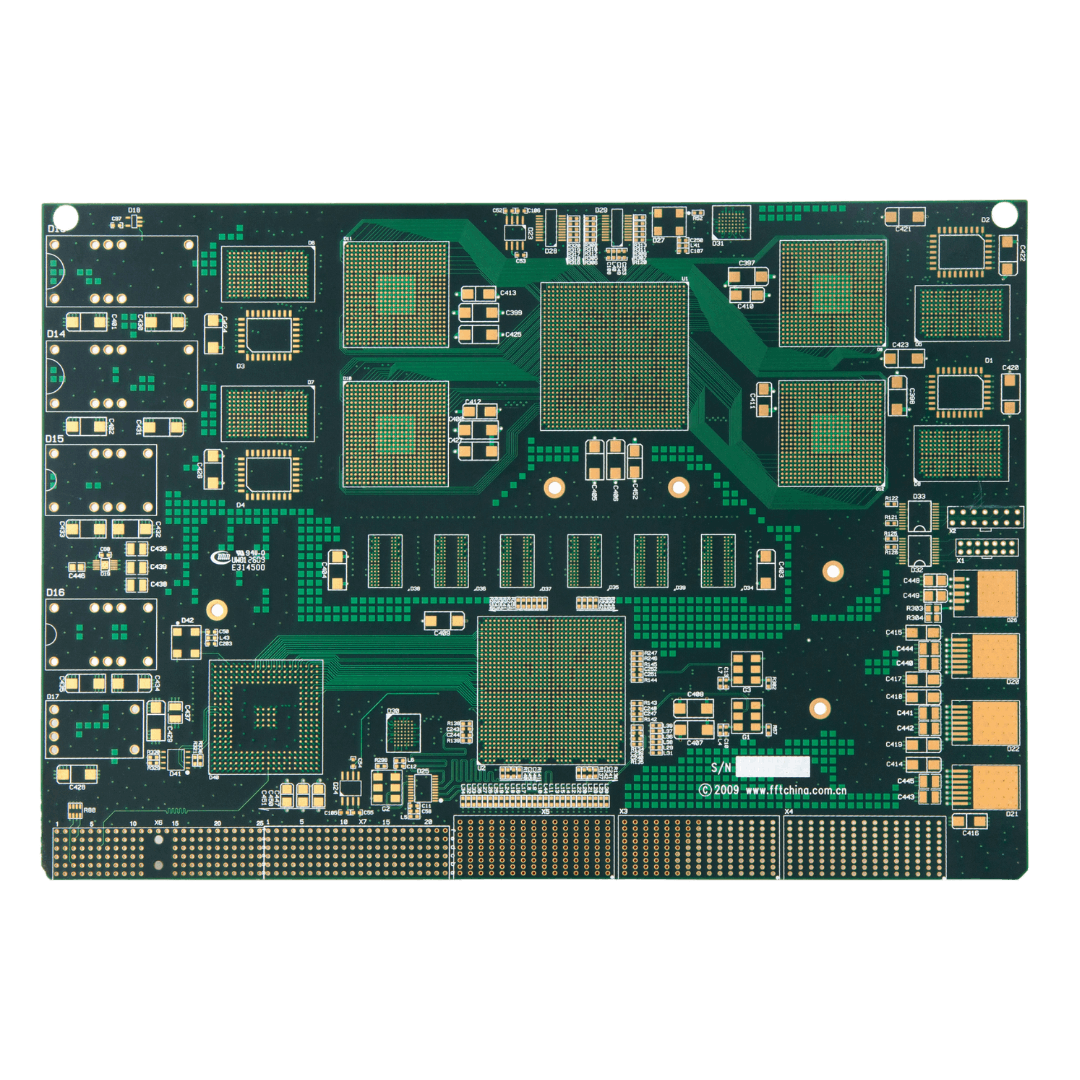

OurPCB offers specialized 14-layer PCB fabrication for the most demanding high-density printed circuit boards. High-layer PCBs require advanced technology and expertise, and our team and factories are ready to manufacture the PCBs you need.


For complex 14-layer PCB fabrication, we offer specialized consultation and a custom timeline for your project. Our extensive manufacturing expertise and certified factories allow us to accommodate high-layer count orders with precision and excellence.

| Specification | PCB Capability |
|---|---|
| Layer Counts | 1-64 layers |
| Lead Time | Normal: 5-6 Days Expedited: 24-48Hours |
| Materials | FR4, Metal Core, Arlon, Taconic, Nelco, Isola, Halogen Free, Rogers, PTFE, PI,etc. |
| Max. Copper | 1000um |
| Finished Board Thickness | 0.1 – 12 mm |
| Size of Finished Products(Max) | 22.5 * 47.2 inch |
| Size of Finished Products(Min) | 2 * 5mm |
| Min. Line/Track Width&Space of Inner Layer | 1.8/1.8 mil |
| Min. Line/Track Width&Space of Outer Layer | 2/2 mil |
| Buried / Blind Via (Non-cross) | 0.1 mil |
| Aspect ratio | 40 : 1 |
| Min. Drilling Size(Mechanical) | 0.1 mm |
| Surface Treatment | HASL, Lead free HASL, ENIG(+ G/F), Immersion silver/Tin, OSP, ENEPIG, bare copper. |
| Wrap and Twist | ≤0.5% |
| Tolerance PTH/ Pressing fit hole /NPTH | ±0.0762 mm /±0.05mm /±0.05mm |
| Drill tolerance | ±2mil |
| BGA pitch | 8mil |
| Layer to layer registration | ±3mil |
| Advanced Via & Hole Structures | Blind/Buried Vias, Via-in-Via, Mechanically Crossed Blind Vias, Stacked Vias, Via-in-Pad |
| Impedance Control | ±5Ω (<50Ω), ±10% (≥50Ω) |
| HDI | 18L any layer HDI (8+N+8 structure) |
| Qualifications | ISO14001:2015, ISO9001:2015, ISO 13485:2016, IATF16949: 2016, Certified |
![]()
![]()
![]()
![]()
OurPCB brings almost 2 decades of multilayer PCB expertise, technical support, and manufacturing capabilities to your most complex printed circuit boards, with a consultative approach to ensure manufacturability and performance. We’re a 14-layer circuit board manufacturer you can trust.

OurPCB’s skilled technicians have years of experience in multilayer PCB manufacturing, allowing us to accommodate specialized 14-layer projects. While extending beyond our standard catalog capabilities, our team’s expertise in providing custom solutions makes us one of the most reliable 14-layer circuit board manufacturers on the market.
Mon-Fri: 24 hours,
Sat: 9am-6pm, GMT+8
Reach us at
[email protected]
24 hours online
+86-199-30589219
Mon-Fri: 24 hours,
Sat: 9am-6pm, GMT+8
Yes, we offer a 14-layer PCB rapid prototyping service with a turnaround time of 120 hours. But complex or large-scale PCBs require custom quoting and project planning as they extend beyond our standard catalog. Please contact us for a consultation to determine specific lead times based on your design requirements.
Yes, we support low-volume prototyping for 14-layer designs. This helps identify performance issues early and confirm manufacturability before scaling.
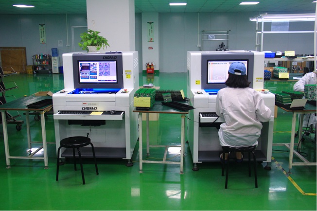
Every 14-layer PCB board undergoes multi-stage inspection, including AOI, X-ray, and final electrical testing. We also offer optional functional testing and first-article reports upon request.
Key considerations include signal integrity management, layer stack-up optimization, thermal management, and via strategy. Our technical team provides consultation on these aspects to ensure manufacturability and performance.
High-layer count PCBs offer more routing space, which supports dense component layouts and complex circuits. They improve signal integrity through dedicated ground and power planes, reduce noise, and ensure clean signal transmission. Multiple layers also help with stable power distribution, making them suitable for advanced systems.
These boards enable compact designs without sacrificing performance, ideal for high-speed, RF, or mixed-signal applications in industries like aerospace, telecom, and medical technology.
Yes, our facilities are certified to manufacture to IPC-A-610 Class 2 and Class 3 standards, which are required for aerospace, medical, and high-reliability applications.
When considering the best places for manufacturing data cables, China immediately comes to mind. It’s no surprise either — the country has rapidly ascended in
Finding the right wiring harness manufacturer for your vintage ride can be a real headache. Those beautiful old machines need special wiring that looks period-correct
Would your car be able to run without wire harnesses? Not a chance. Wire harnesses connect all the electrical parts together. No harness means no
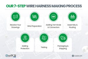
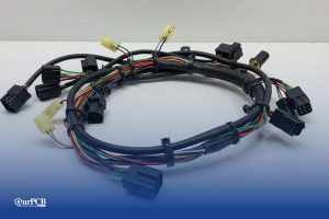
Making wire harnesses isn’t complicated. At OurPCB, we create custom wire harnesses for an expansive range of industries every day. While it’s a complicated process,

Prototype cable assemblies are the very important place in between PCB design ideas and interconnects. OurPCB brings prototype assemblies with PCB solutions to your tables.
PCB thermal management prevents component overheating through strategic heat transfer techniques. Without proper thermal control, electronics are at risk of electronic failures through weakened solder
We use cookies to improve your browsing experience, which may include personal information. By clicking "Agree," you accept our Privacy Policy and cookie use. You can change your cookie settings in your browser anytime.
Agree
 Chat With Us
 Free Quote