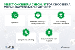
Top 10 Classic Car Wiring Harness Manufacturers | Full Guide
Finding the right wiring harness manufacturer for your vintage ride can be a real headache. Those beautiful old machines need special wiring that looks period-correct

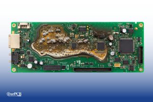
At OurPCB, we offer expert PCB cloning services for clients who need precise duplication of existing circuit boards. Whether you’re looking to clone PCB designs or replicate a fully functioning board, our team ensures high-quality, accurate reproduction. We use advanced techniques to copy your PCB, preserving its functionality, layout, and design.


A PCB clone, also known as PCB duplication or PCB copy, is a replica of an existing circuit board, typically created through reverse engineering. This process is crucial for companies needing to replicate an exact PCB design or reuse parts of a board for different applications. It’s the fastest way to clone PCB design, making it ideal for businesses requiring quick, cost-effective solutions for circuit board reproduction.
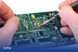
A PCB cloning service allows you to replicate the design of an existing PCB without going through the entire design process. This service is cost-effective and efficient, especially when using PCB clone software to produce precise copies of the circuit board for testing or client samples.


Cloning PCBs comes with multiple benefits and purposes for your company. Here are a few advantages of PCB clones:
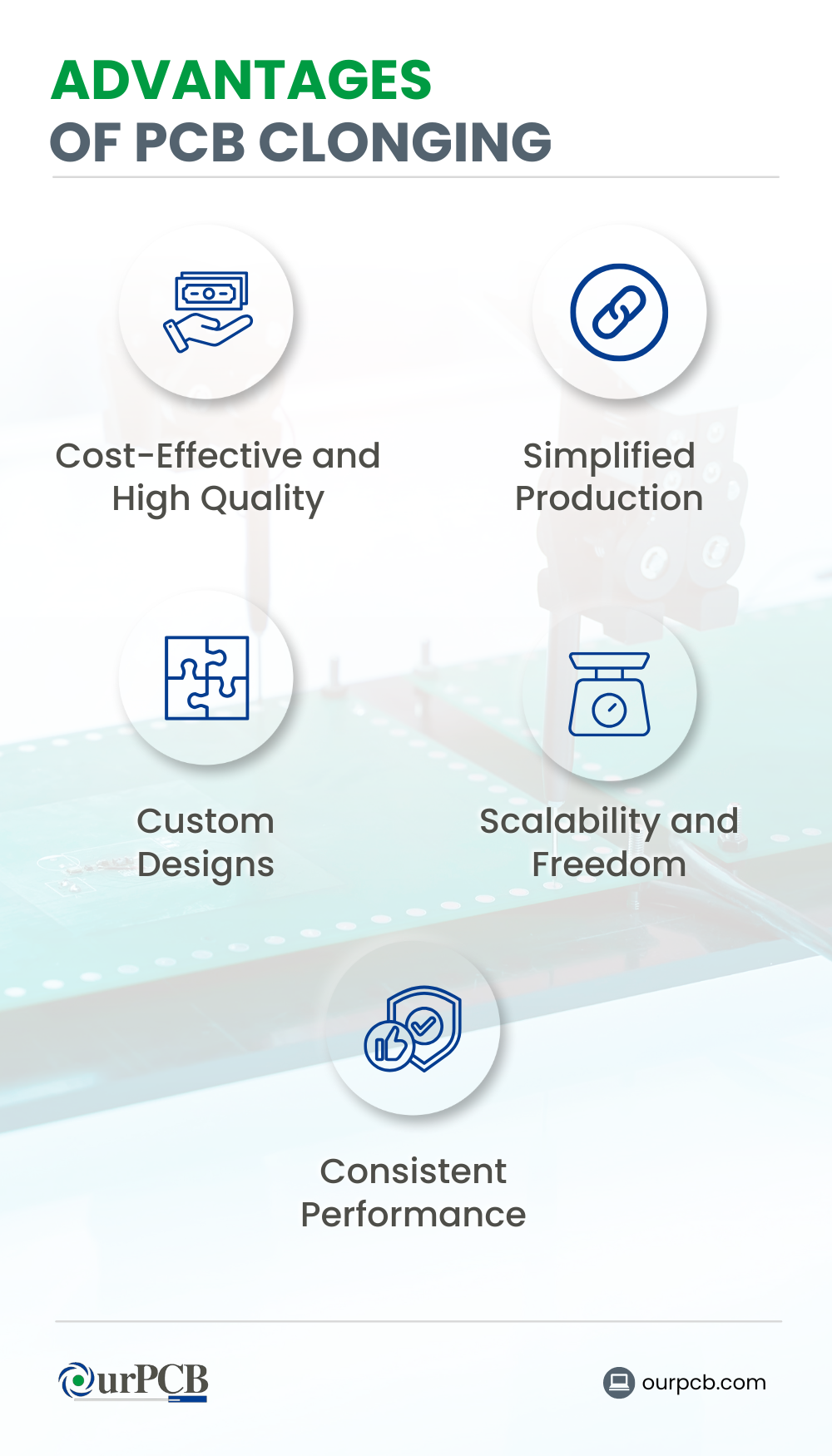

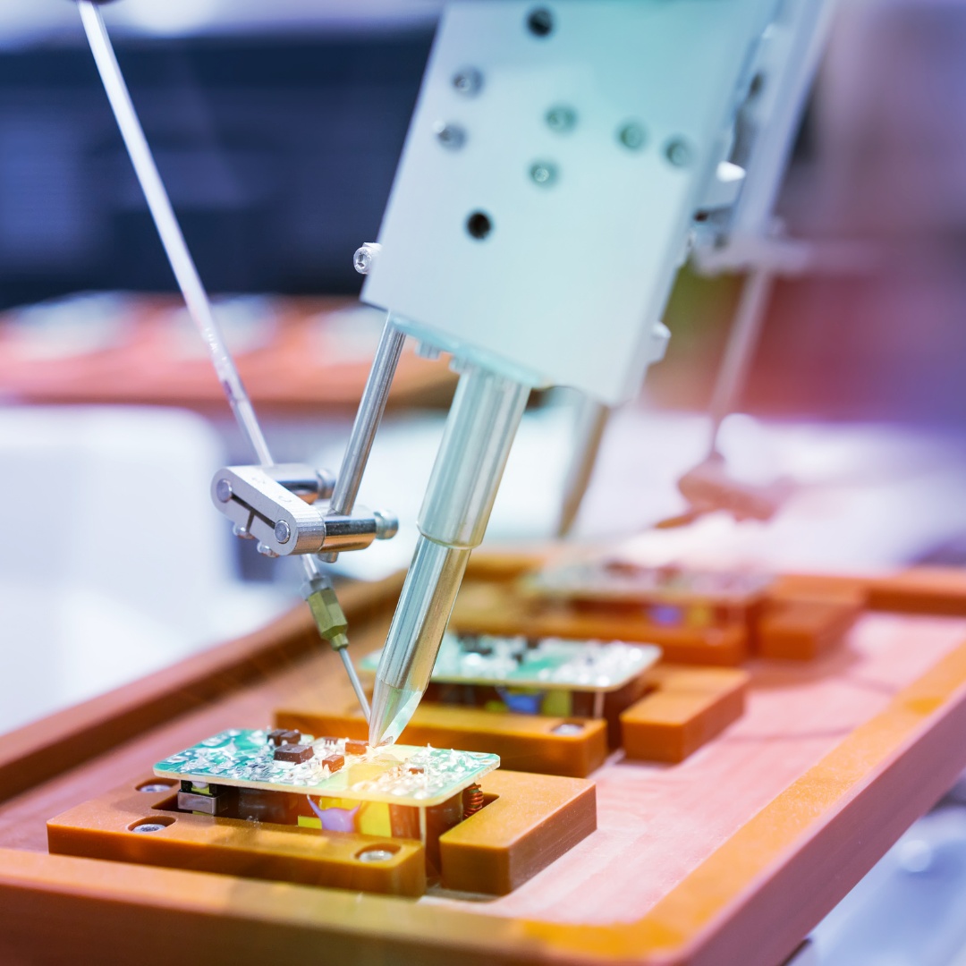
PCB manufacturing can be time-consuming and expensive, but PCB clones provide a cost-effective alternative without compromising quality. With PCB duplication, you save on testing, prototyping, and design costs, reducing both development time and expenses. By streamlining the process, PCB clones ensure consistent quality while allowing faster time to market and lower overall costs.
Companies looking to adopt advanced technologies must thoroughly analyze their PCBs. Our analysis helps engineers create high-quality designs by ensuring optimal performance and reliability. With the right techniques, engineers can also construct temperature-reliable PCBs that meet industry standards for durability and efficiency.
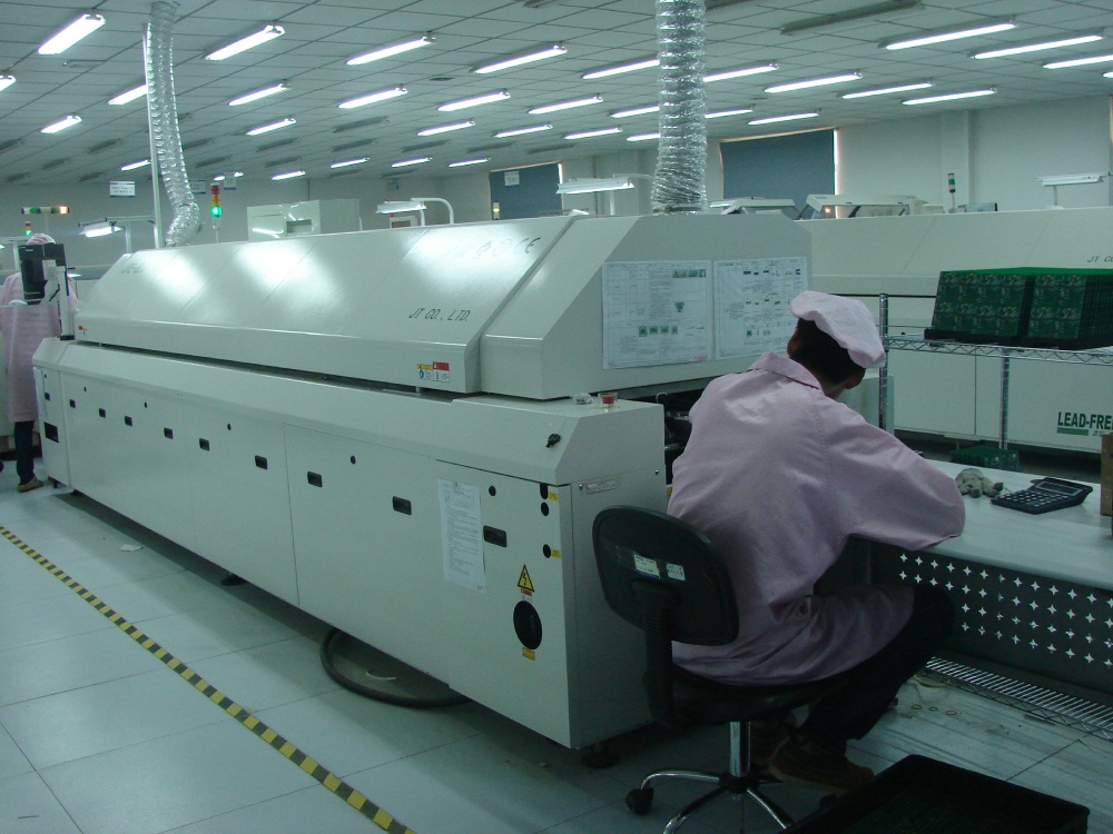
PCB cloning automates much of the production process, making it ideal for replacing obsolete PCBs in electronic products. Manufacturers use reverse engineering to identify innovative designs, which are then used to create new PCBs. This streamlined process reduces production time and ensures the new board matches the original’s functionality.
Cloning PCBs allows you to modify designs to meet the specific requirements of your components. You can also create entirely unique products or update an existing design to suit new needs. Custom designs make it easier to adapt to technological advancements or market demands, offering greater flexibility in your product development.
PCB cloning enables mass production from a single design, resulting in multiple PCB copies. The flexibility in manufacturing ensures that each PCB assembly can be tailored to the customer’s needs. This scalability offers businesses greater freedom to meet specific production demands while maintaining high standards.
PCB cloning ensures that cloned boards maintain the same performance standards as the originals. The mechanical and electrical properties of the cloned PCBs make them ideal for high-performance applications, ensuring they meet the required specifications for reliability and longevity in critical environments.

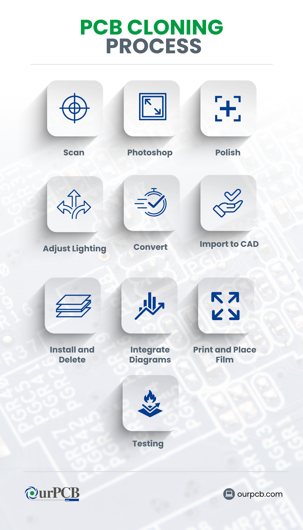
Let’s get into how to copy a PCB! Make sure to follow these steps when cloning PCB:
Remember, you need to focus on completing a successful PCB copy with the correct methods. Usually, an experienced PCB clone servicer normally carries out the process, but you can too!
You might be wondering, “Is PCB cloning legal?”
Since the start of reverse technology, a lot of doubts have ensued. Its legitimacy has constantly been in question for a long time.
For example, the court in China around January 2007 stipulated that trading information gained from reverse engineering was irrelevant. Thus, this meant that reverse engineering violated trade secrets and was hence inappropriate.
However, in the following month, the court revisited the case. Now, engineering services play a vital role in circuit industry development. However, its legitimacy is still in question.
Currently, most companies have rules on the issue. For example, anyone who wants to use reverse engineering must own design copyrights. This is necessary for legal purposes. The copyright protects the interests and legitimacy of the original designer.
PCB cloning makes work easier, cuts costs, and increases PCB production capacity. Most manufacturers prefer cloning to construct a PCB schematic diagram from scratch. Before trying PCB cloning, you should understand its procedures, advantages, and legal considerations.
We truly hope this article has been beneficial to you. For any further questions regarding PCB cloning, do not hesitate to contact us. Our friendly team are more than willing to help you!
We handle everything from parts sourcing to final assembly, providing a hassle-free experience that ensures top-quality boards every time.
Whether you need a few prototypes or large-volume batches, our flexible assembly services adapt to your project’s scope and timeline.
Stay environmentally responsible with our compliant assembly processes, offering RoHS and lead-free options for safe, reliable builds.
No matter the complexity, we can assemble boards of all configurations—single-layer, multi-layer, or a mix—to match your exact specifications.
From one-off prototypes to bulk orders, we accommodate projects of all sizes without compromising on quality or turnaround time.
Join our growing community of satisfied clients who rely on our dependable assembly expertise and dedicated customer support.
Mon-Fri: 24 hours,
Sat: 9am-6pm, GMT+8
Reach us at
[email protected]
24 hours online
+86-199-30589219
Mon-Fri: 24 hours,
Sat: 9am-6pm, GMT+8
The main difference between a PCB and a microchip is that PCBs enable connectivity between electronic components, while a microchip analyses data and sends out instructions. PCBs are boards with multiple components, including microchips.
FR-4 is one of the cheapest PCB materials. It’s from woven glass fiber and epoxy resin. While it is cost-effective, it still has great mechanical strength and insulation.
Finding the right wiring harness manufacturer for your vintage ride can be a real headache. Those beautiful old machines need special wiring that looks period-correct
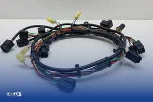
Would your car be able to run without wire harnesses? Not a chance. Wire harnesses connect all the electrical parts together. No harness means no
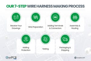
Making wire harnesses isn’t complicated. At OurPCB, we create custom wire harnesses for an expansive range of industries every day. While it’s a complicated process,

Prototype cable assemblies are the very important place in between PCB design ideas and interconnects. OurPCB brings prototype assemblies with PCB solutions to your tables.
PCB thermal management prevents component overheating through strategic heat transfer techniques. Without proper thermal control, electronics are at risk of electronic failures through weakened solder
ContentsKey TakeawaysWhat is a Multilayer-Printed Circuit Board?How do Multilayer PCB Boards Work?Multilayer PCB ApplicationsMultilayer PCB Manufacturing Process: StepsMultilayer PCB Manufacturing MachinesBenefits of Multilayer Circuit BoardsWhat
We use cookies to improve your browsing experience, which may include personal information. By clicking "Agree," you accept our Privacy Policy and cookie use. You can change your cookie settings in your browser anytime.
Agree
 Chat With Us
 Free Quote