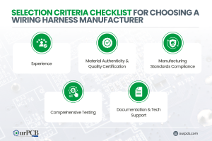
Top 10 Classic Car Wiring Harness Manufacturers | Full Guide
Finding the right wiring harness manufacturer for your vintage ride can be a real headache. Those beautiful old machines need special wiring that looks period-correct

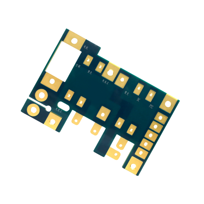
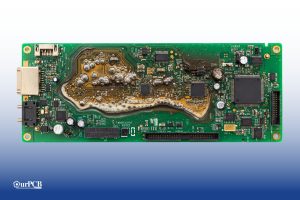
As a trusted 8-layer PCB manufacturer, we build multilayer circuit boards with eight copper layers stacked for compact routing, stable signal flow, and reliable performance in high-density electronics.


OurPCB specializes in high-precision 8-layer PCB stack-up fabrication with superior quality control and competitive lead times. Our advanced facilities deliver complex multilayer circuit boards for demanding applications across multiple industries. We’re your one-stop shop for all things PCB, streamlining the supply chain and speeding up your entire process.


With specialized equipment and extensive expertise in multilayer technology, OurPCB delivers premium 8-layer PCBs with precise impedance control, advanced material options, and comprehensive testing to ensure optimal performance.

OurPCB combines technical expertise in multilayer PCB manufacturing with premium, globally sourced materials and strict quality control to deliver reliable 8-layer PCBs for complex electronic applications.

OurPCB combines technical expertise in multilayer PCB manufacturing with premium, globally sourced materials and strict quality control to deliver reliable 8-layer PCBs for complex electronic applications.
OurPCB combines technical expertise in multilayer PCB manufacturing with premium, globally sourced materials and strict quality control to deliver reliable 8-layer PCBs for complex electronic applications.
OurPCB employs advanced manufacturing techniques including precise layer alignment, sophisticated lamination processes, and automated optical inspection to ensure consistent quality across every 8-layer PCB stack-up.

Mon-Fri: 24 hours,
Sat: 9am-6pm, GMT+8
Reach us at
[email protected]
24 hours online
+86-199-30589219
Mon-Fri: 24 hours,
Sat: 9am-6pm, GMT+8
Lead times for 8-layer PCBs depend on the processing area: 7 days for areas <1m², 12 days for 1m² to 3m², 20 days for 3m² to 30m², and 25 days for areas >30m².
OurPCB offers FR4, High TG FR4, halogen-free materials, and Rogers HF materials for high-quality 8-layer boards, depending on your specific application requirements.
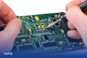
Yes, we offer complete assembly services for 8-layer PCBs, including component sourcing, placement, soldering, and comprehensive testing to ensure functionality.
Our 8-layer PCBs meet ISO9001:2015, ISO13485:2016, IATF 16949:2016, and IPC-A-610 Class 2 & 3 standards with rigorous quality control throughout the manufacturing process.
Yes, our technical support services for multilayer boards include PCBA review, impedance matching calculation, and design recommendations to optimize your 8-layer PCB performance and manufacturability.
8-layer PCBs present several challenges, starting with signal integrity concerns due to tighter spacing and increased risk of crosstalk and EMI. Precise layer alignment during lamination is necessary to avoid defects, which makes manufacturing more complex.
These boards also generate more heat, so thermal management and material choice become more serious design factors. Routing across eight layers requires detailed planning to maintain impedance and reduce interference. As a result, both production costs and turnaround times are higher compared to simpler PCB designs.
Finding the right wiring harness manufacturer for your vintage ride can be a real headache. Those beautiful old machines need special wiring that looks period-correct
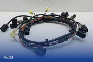
Would your car be able to run without wire harnesses? Not a chance. Wire harnesses connect all the electrical parts together. No harness means no
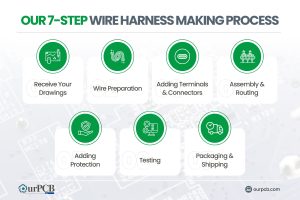
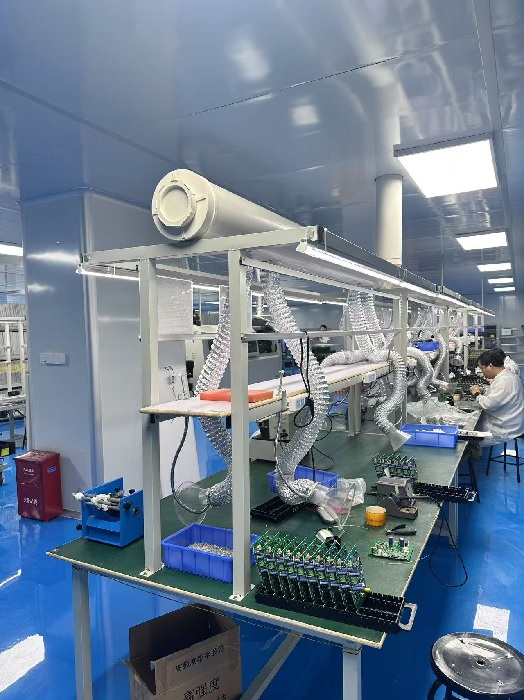
Making wire harnesses isn’t complicated. At OurPCB, we create custom wire harnesses for an expansive range of industries every day. While it’s a complicated process,
Prototype cable assemblies are the very important place in between PCB design ideas and interconnects. OurPCB brings prototype assemblies with PCB solutions to your tables.
PCB thermal management prevents component overheating through strategic heat transfer techniques. Without proper thermal control, electronics are at risk of electronic failures through weakened solder
ContentsKey TakeawaysWhat is a Multilayer-Printed Circuit Board?How do Multilayer PCB Boards Work?Multilayer PCB ApplicationsMultilayer PCB Manufacturing Process: StepsMultilayer PCB Manufacturing MachinesBenefits of Multilayer Circuit BoardsWhat
We use cookies to improve your browsing experience, which may include personal information. By clicking "Agree," you accept our Privacy Policy and cookie use. You can change your cookie settings in your browser anytime.
Agree
 Chat With Us
 Free Quote