Circuit board building occurs in two primary stages: fabrication/ manufacturing and assembly. While it is possible to do the quick turn pcb assembly process manually, it can lead to several mistakes, and the slow speed is not feasible for commercial production. Therefore, you will need to employ assembly machines for this task. But how will these machines know where to place the components? That is where fiducial PCB marks come in. Here's a detailed explanation of how these marks assist the assembly machines.
Contents
- What Are Fiducial PCBs?
- Types of PCB Fiducial Marks
- Panel Marks
- Component (Local)
- Board (Global)
- Structure of Fiducial Markers
- Fiducial Mark Construction
- Positional Accuracy
- Contrast
- Flatness & Edge Clearance
- How Machines Use Fiducial Marks
- When To Use Fiducial Marks
- PCB Fiducial Marker Placement Guidelines
- Select the Fiducial Marker Type
- Identify Where To Place the Marker
- Determine the Best Fiducial Shape and Size
- Determine How Many Fiducial Points To Use
- Consult Your PCB Assembler
- Wrap Up
What Are Fiducial PCBs?
In a nutshell, fiducial PCB marks are alignment marks used by surface mount assembly machines to place electronic components on the board.
Fiducial refers to a fixed reference point used for comparison purposes. Therefore, fiducial markers are surface marks used for indexing systems as directional measures.
In electronics, fiducial marks are alignment marks that assist the indexing system with board orientation in automated pick-and-place machines. They help the equipment to keep the board aligned as close to perfect as possible for precise placement.
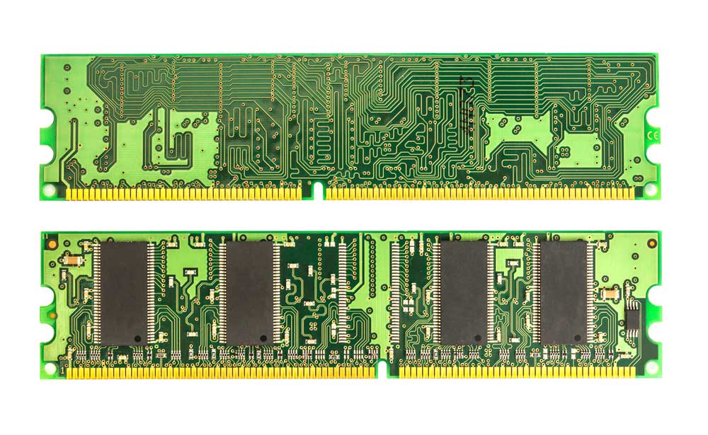
A DDR4 RAM PCB with three fiducial marks
The assembly machinery uses cameras to spot these marks, then make necessary adjustments for correct orientation.
Types of PCB Fiducial Marks
The copper pad of a fiducial PCB mark should be circular. But the cutout can be in any shape, most being diamond-shaped or square. Regardless of the form, these markings fall into the following categories.
Panel Marks
Panel marks lie on the four outermost corners to ensure proper panel alignment.
Component (Local)
These copper markers sit outside quad-packaged surface-mount components to help locate a component's footprint precisely.
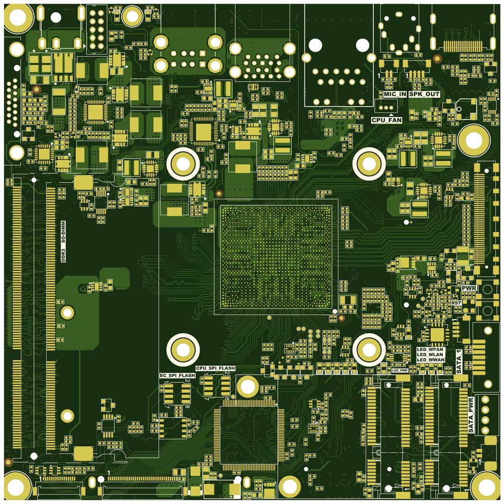
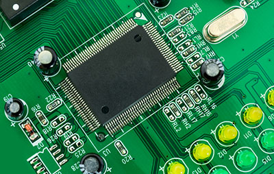
A blank PCB ready for SMT component assembly
Board (Global)
Global markings define the board edge clearance perimeter and the circuit board's exterior. Usually, they have a three-grid positioning system where the reference point (0,0) is at the lower left end, while the other two points are in the positive direction of the X and Y axis. This arrangement helps the placement machinery calculate the board's orientation in the X and Y axis.
Structure of Fiducial Markers
Each fiducial marker is a solid copper mark with a minimum diameter of 1mm and a maximum of 3mm. Points on the same board cannot vary size-wise by more than 25 microns. And they should be clear of any solder mask, circuit pattern/feature, or other markings.
Assemblers usually prefer a clear area around the fiducial spot equal to its diameter, but the minimum clear area should be at least equal to its radius.
Special Offer: Get $100 off your order!
Email [email protected] to get started!
Fiducial Mark Construction
Consider the following factors when constructing fiducial markers.
Positional Accuracy
A PCB fiducial must sit on the copper layer that holds all SMT components. This copper layer gets placed in one operation, meaning the positional accuracy of the surface-mount pad relative to the copper fiducial will remain constant.

SMT components positioned accurately on a PCB
Don't use silk screen patterns or drill holes as fiducial markers because they get added in separate operations. Their registration will vary depending on the board, resulting in lower positional accuracy.
Contrast
Cameras in the machine assembly process require high contrast to identify the reference mark. Therefore, this point has to contain bare copper without a silkscreen or solder mask above it.
A circuit board with two clear circular fiducial markers
The copper pad fiducial diameter can be 1-2mm with nickel or tin plating and transparent anti-oxidation or solder coating. And the mask opening can be 2-5mm larger than the pad size.
Flatness & Edge Clearance
The fiducial marker's surface flatness should be lower than 15 micrometers. And its location to the edge should be at least 7.62mm plus the fiducial clearance.
How Machines Use Fiducial Marks
Assembly machines use high-tech cameras to detect these pads. The first fiducial enables the equipment to notice a board's presence and give it a datum/reference point.
The second mark enables the vision system to identify the circuit pattern orientation on the board. Also, it helps determine if the board has a skewed pattern when placing it on the machine's clamps.

A pick-and-place machine assembling components on a PCB
Lastly, the third mark allows the calculation of the stretch shrink on the board and circuit pattern. This calculation comes in handy when dealing with large PCBs because the tiny variations add up to a significant value over a long distance. These variations can interfere with the component placement accuracy at the board's tail end.
This third marker also comes in handy when dealing with dual-sided SMT assemblies because reflowing one side causes stretching, bowing, flexing, and shrinking. The calculation helps compensate for these factors when placing components on the other side.
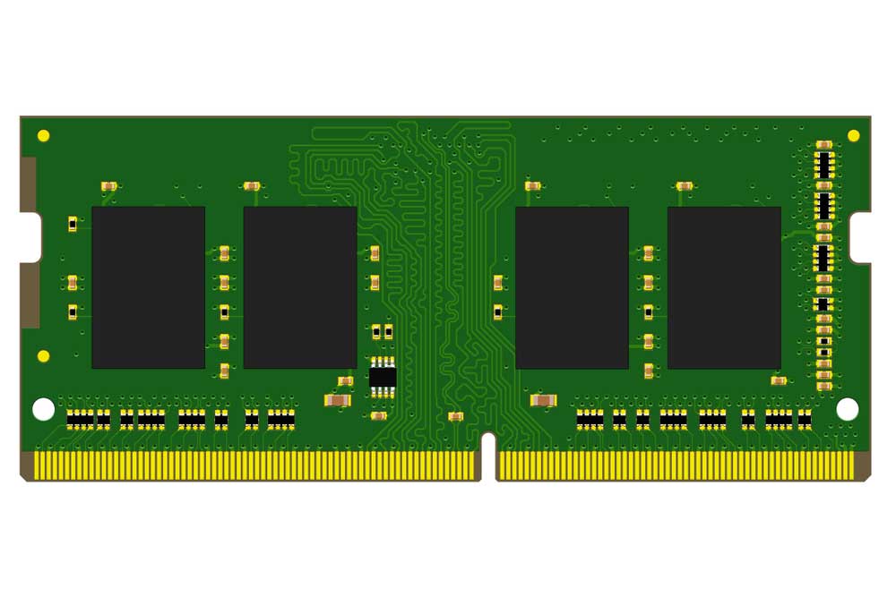
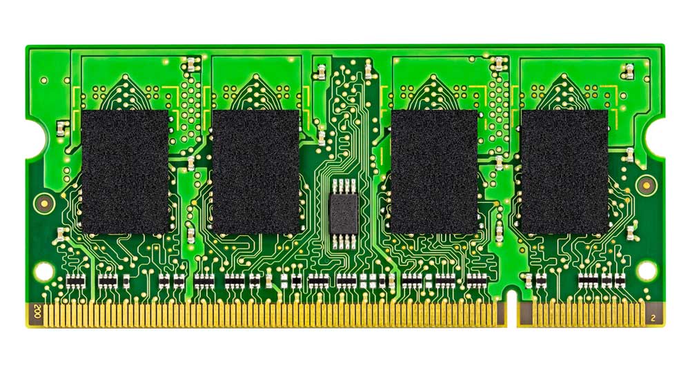
A computer memory card with three fiducial markers
When To Use Fiducial Marks
Always use fiducial markers in a high-volume assembly line for precise registration and component placement. They might not be necessary for low-volume assembly lines, but some of these assemblers rely on them. The only instance when these pads are not vital is if you are placing the components by hand.
PCB Fiducial Marker Placement Guidelines
Use the following guidelines to maximize the effectiveness of fiducial markers during assembly.
Select the Fiducial Marker Type
The panel, local, and global fiducial markers have similar purposes but vary in number, shape, and location. So select the most suitable type first.
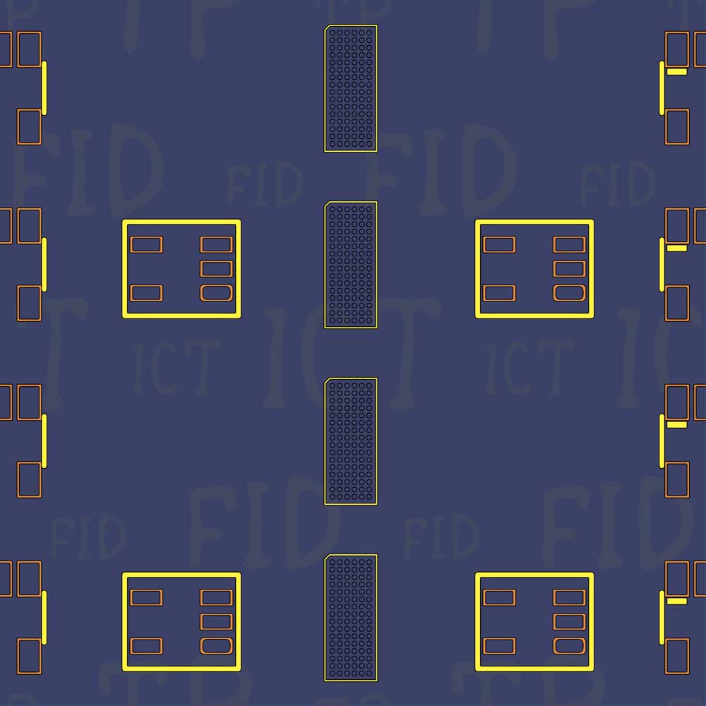
An abstract PCB design showing how an assembly machine would place SMT components
Identify Where To Place the Marker
Corner locations are better for global and panel fiducial marks because they give proper edge clearance. And place one pad next to each SMT component.
Determine the Best Fiducial Shape and Size
The typical mask opening diameter for the PCB fiducial is 2mm and 1mm for the copper diameter. But you can consult the IPC guidelines on the mark's clearance, shape, and size.
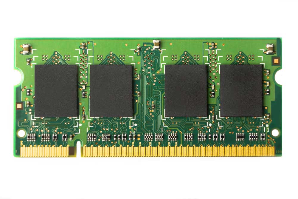
An assembled RAM module with square fiducial marks
Determine How Many Fiducial Points To Use
There is no predefined number of fiducial marks for a PCB. But the general rule of thumb is to have a minimum of one for the local marking, two for global markings, and three for panel markings.
Consult Your PCB Assembler
Always consult your PCB assembler for the fiducial parameters that optimally align with their assembly equipment. We do PCB fabrication and assembly, so we can help you with your designs to create an optimal layout for all the manufacturing and assembly processes.
Wrap Up
To conclude, fiducial markers are essential in automated assembly processes because they ensure that pick-and-place machines function precisely. Therefore, you should use the guidelines above to design and position them accurately or contact us for guidance on designing these copper pads on your PCB.
Special Offer: Get $100 off your order!
Email [email protected] to get started!