Contents
- Typical PCB Panel Sizes
- How is PCB Thickness Measured?
- What Factors Influence PCB Thickness?
- 1. Material Choice
- 2. Copper Thickness
- 3. Prepreg and Dielectric Materials
- 4. Number of Layers
- 5. Environmental Factors
- Why is PCB Thickness Important in Design?
- Electrical Performance
- Mechanical Stability
- Thermal Management
- Ease of Component Assembly
- How Does the Thickness of PCBs Affect Manufacturing?
- Drilling Equipment Limitations
- Recanalization Techniques
- How to Choose the Right PCB Thickness
- Weight Considerations
- Assembly Components Requirements
- Specific Application Needs
- Electrical Requirements
- Physical Space Constraints
- Using a Trace Width Calculator
- PCB Thickness Management: Challenges and Solutions
- Warping
- Uneven Thickness
- Manufacturing Inconsistencies
- How Does PCB Thickness Impact Cost?
- Material Costs
- Manufacturing Processes
- Design Considerations
- Thermal Management
- Application-Specific Needs
- Economies of Scale
- When Should Custom PCB Thickness Be Considered?
- Key Considerations for Custom-Thickness PCBs
- How Are Custom-Thickness PCBs Manufactured?
- PCB Thickness FAQs
- Can PCB Thickness Affect Electromagnetic Interference (EMI) Performance?
- What Are the Common Applications for Ultra-Thin PCBs?
Typical PCB Panel Sizes
Panel Sizes
PCBs are produced in panels to maximize the efficient use of standard laminate materials. The most common panel size is 18” x 24”, providing a usable area of 16” x 22”. Other standard panel sizes include:
- 21” x 24”
- 24” x 32”
- 24” x 30”
- 16” x 18”
Importance of Panel Sizes
Understanding optimal panel sizes is essential for PCB designers to ensure dimensions are adjusted for efficient material usage. Using larger panel sizes may restrict the number of fabricators available due to specialized tooling requirements. For more insights into optimizing dimensions and layout, explore the benefits of PCB panelization to streamline manufacturing and reduce costs.
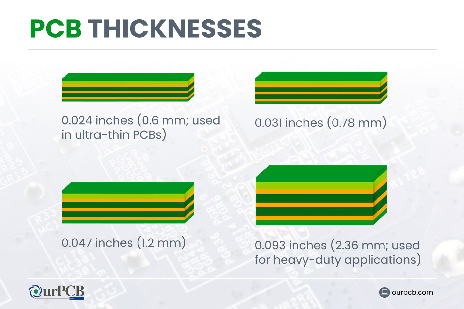
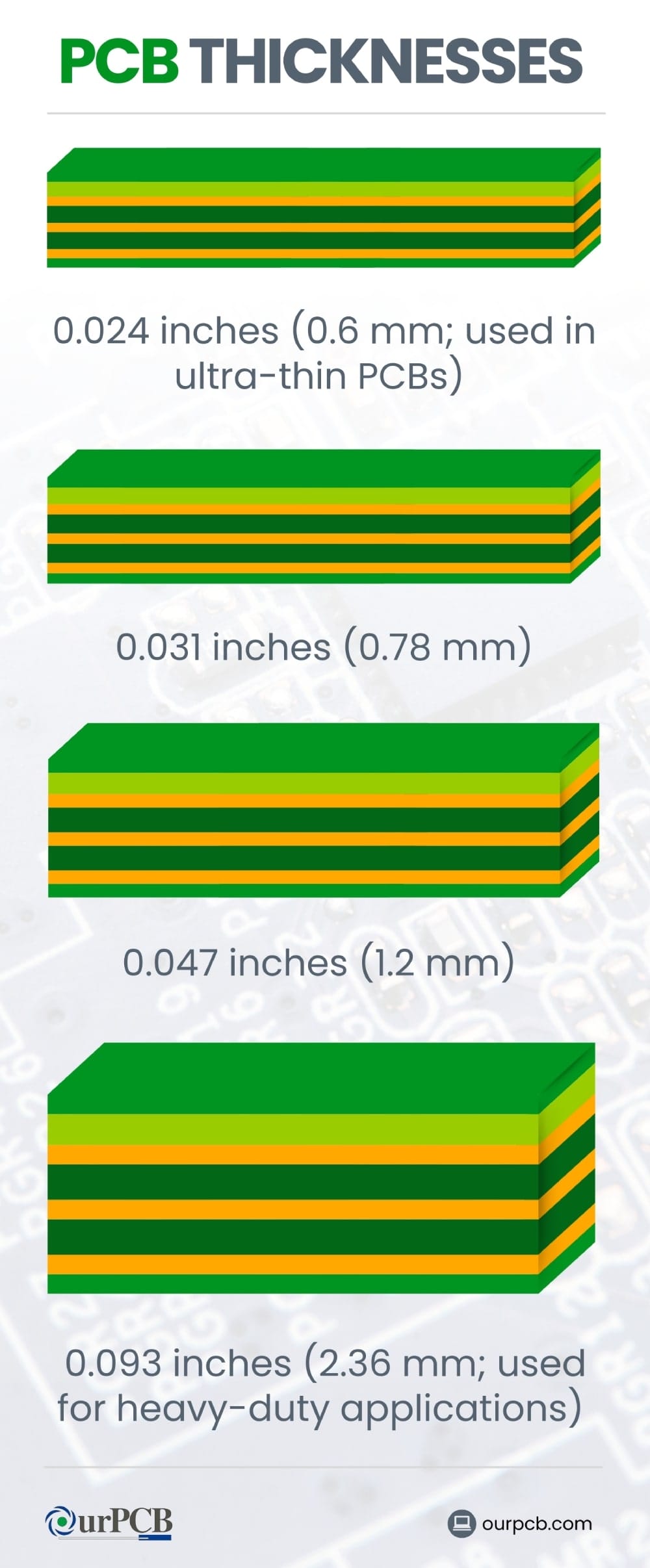
How is PCB Thickness Measured?
PCB is measured using precise tools and techniques, including:
- Micrometer: This tool provides highly accurate measurements by making physical contact with the PCB. It’s often used for spot-checking PCB thickness.
- Calipers: These provide a quick and relatively accurate measurement of the PCB thickness. Digital calipers offer easier reading and more precise measurements.
- Non-Contact Methods: Advanced techniques like laser micrometers and optical profilers measure thickness without touching the PCB. This is useful for delicate or flexible PCB boards.
What Factors Influence PCB Thickness?
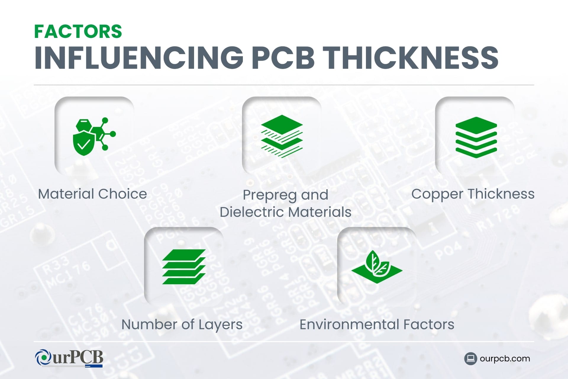
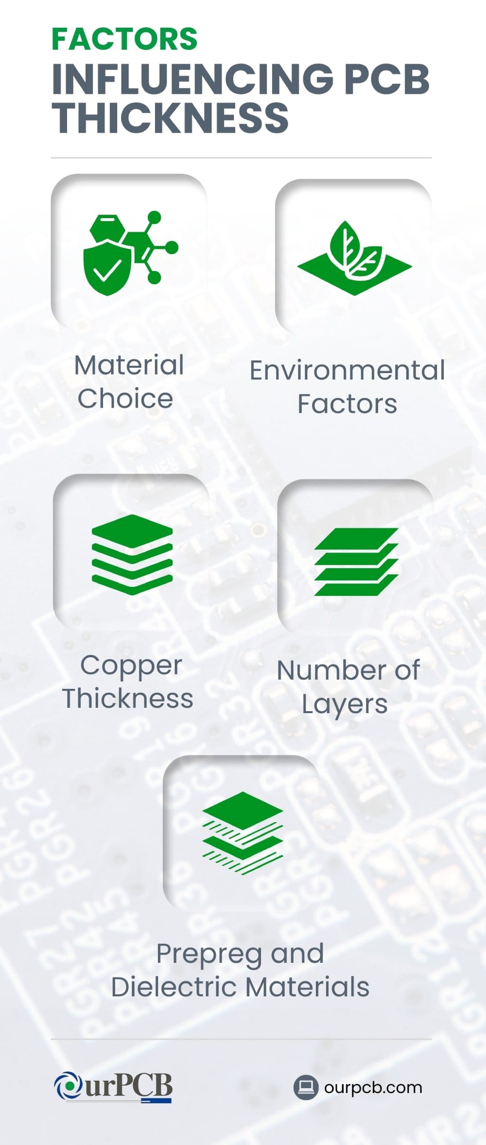
Several factors can significantly influence circuit board thickness, impacting their design, performance, manufacturability, and reliability.
1. Material Choice
Common substrate materials like FR-4 come in a range of thicknesses, typically ranging from 0.2 mm to 3.2 mm. The choice of circuit board material is determined by factors like thermal and mechanical properties, dielectric constant, and cost.
2. Copper Thickness
Copper thickness determines the PCB’s current-carrying capacity and thermal performance. Common copper thicknesses fall between 1.4 and 2.8 mm, with higher thicknesses used for high-power applications or improved heat dissipation.
Additionally, copper thickness is often measured in ounces per square foot. You may see common copper thicknesses of 0.5 oz, 1 oz, and 2 oz. To explore how different copper weights impact PCB design and performance, learn more about copper PCBs and their applications in various industries.
3. Prepreg and Dielectric Materials
These are insulating layers, or dielectric materials, used between the copper layers in multilayer PCBs. The materials range from 0.1 mm to 0.4 mm thick. The choice of dielectric material impacts the PCB’s impedance, signal speed, and thermal expansion properties. For demanding applications like high-temperature or high-frequency designs, consider the benefits of polyimide PCBs, known for their superior thermal and electrical properties.
4. Number of Layers
Single-layer PCBs typically have a standard thickness of around 1.6 mm, while multilayer PCBs can be several millimeters thick. Multilayer PCB thickness will also depend on the number of conductive and insulating layers.
5. Environmental Factors
In harsh environments, like those with high temperatures, humidity, or mechanical stress, thicker PCBs are preferred for their durability and reliability. Thicker boards provide better thermal management and mechanical strength, making them suitable for applications in industries like automotive, aerospace, and industrial control.
Why is PCB Thickness Important in Design?
Printed circuit board thickness affects various aspects of the board’s performance and durability. As each project is unique and requires different PCB thicknesses, choosing the right thickness means that the PCB can handle the electrical, mechanical, and thermal demands of the application. Here’s why it’s important:
Electrical Performance
The thickness of a PCB influences its electrical characteristics, including impedance, signal integrity, and the ability to carry current. Thicker boards can support higher current loads. They also help reduce the resistance of the circuit, which can improve overall performance.
Proper thickness means signals can be transmitted without distortion, which is especially important for high-frequency applications like RF and microwave circuits. To delve deeper into the relationship between trace width, thickness, and signal transmission, explore PCB transmission lines and their role in optimizing performance.
Mechanical Stability
Thicker boards provide greater rigidity, making them less prone to bending or warping. This rigidity is handy for boards that will be subject to mechanical stress or vibration, like those used in automotive or industrial applications. For designs that require both flexibility and mechanical strength, learn more about what is rigid-flex PCB and how it combines stability with adaptable form factors to meet complex requirements.
Thermal Management
Thicker boards can dissipate heat more effectively, which is a must for high-power applications. Proper heat dissipation prevents overheating and extends the lifespan of the components. Thicker copper layers within the PCB can enhance thermal conductivity, which ensures heat is spread evenly across the board and away from critical components.
Ease of Component Assembly
Thicker boards can support heavier components and provide a more robust platform for mounting them. This is especially important in designs with large or high-density components that need additional support.
However, designers must balance thickness with the need for precise drilling and etching, as overly thick boards can complicate these processes and increase manufacturing costs.
How Does the Thickness of PCBs Affect Manufacturing?
Thicker PCBs offer increased mechanical strength and better heat dissipation, but they need more material and processing time, leading to higher costs. On the other hand, thinner PCBs are easier and cheaper to produce but can be more fragile and prone to defects. Here are some possible limitations due to PCB thickness:
Drilling Equipment Limitations
Drilling is a key step in PCB manufacturing, and the equipment used has limitations based on the board’s thickness. For thicker PCBs, more precise drilling is needed to avoid damaging the board material.
The depth and diameter of the holes must be accurately controlled, which can be challenging for thicker boards. Also, drilling through multiple layers needs more sophisticated equipment and techniques. This increases the complexity and cost of production.
Recanalization Techniques
Recanalization is the process of separating individual PCBs from a larger panel. Common techniques include V-scoring, tab routing, punching, laser cutting, and water jet cutting.
Each method has its advantages and limitations, depending on the PCB’s thickness and design requirements. For instance, V-scoring is cost-effective but may not be suitable for thicker boards, while laser cutting offers high precision and clean edges but is more expensive.
Special Offer: Get $100 off your order!
Email [email protected] to get started!
How to Choose the Right PCB Thickness
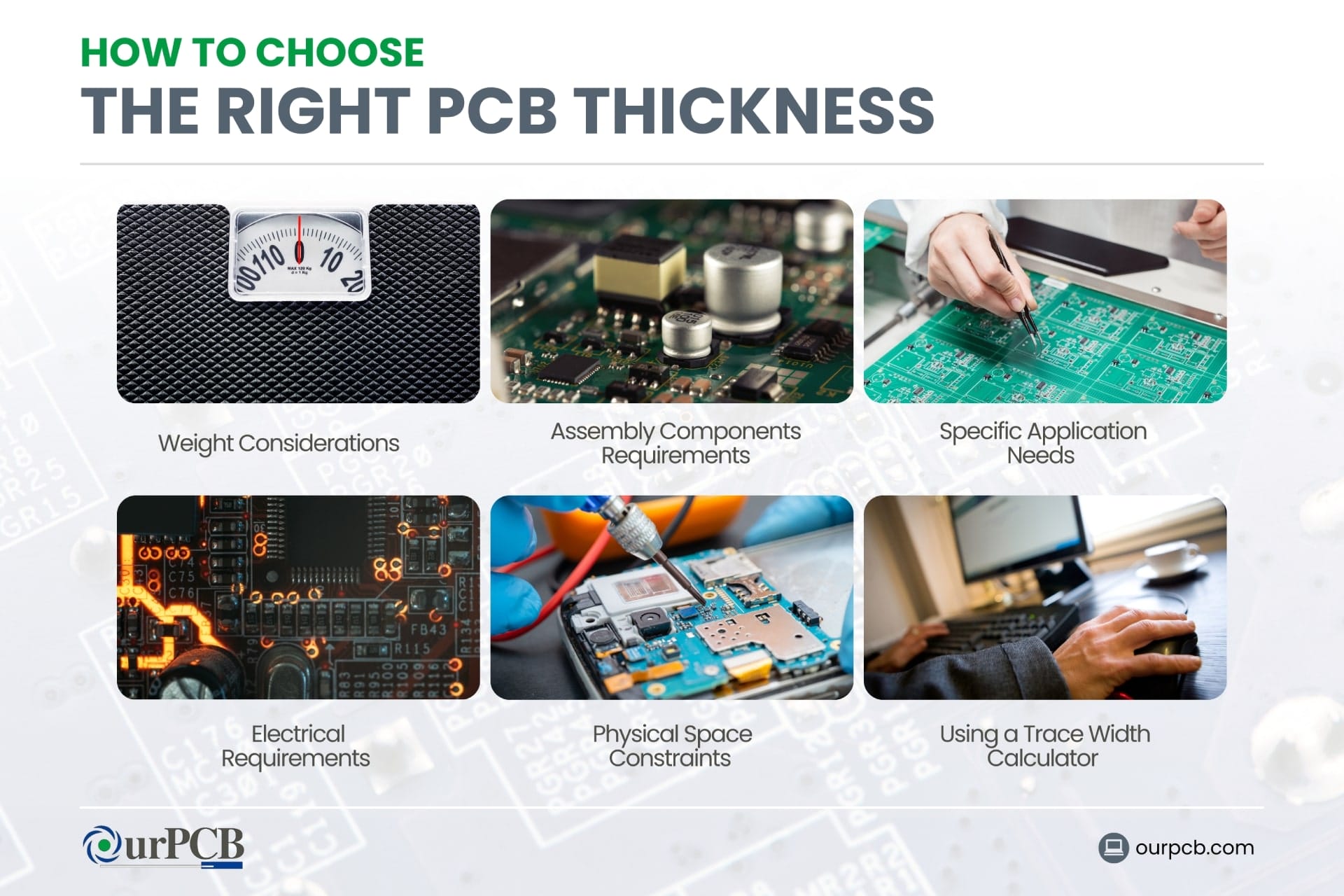

Weight Considerations
The weight of a PCB is directly related to its thickness. Thicker PCBs are heavier, which might be a disadvantage in portable devices such as smartphones, tablets, and wearable technology.
In applications where stability and durability are key, like automotive or industrial equipment, a heavier, thicker PCB may be preferable. Balance the need for strength and durability with the need to keep the overall weight of the device manageable.
Assembly Components Requirements
Some components, like large connectors or heat sinks, may need a thicker PCB to provide support and prevent bending. Plus, the soldering process can be affected by the PCB thickness. Thicker PCBs may need more heat during soldering, which could impact the choice of solder materials and techniques.
Specific Application Needs
Different applications have unique requirements that can dictate the optimal PCB thickness. For example, high-frequency RF and microwave circuits often use thinner PCBs to reduce signal loss and improve performance. On the other hand, PCBs used in power electronics might be thicker to handle higher current loads and provide better thermal management.
Electrical Requirements
Thicker PCBs can support higher current capacities, which is key for power distribution and high-power applications. Also, the impedance of the PCB traces can be affected by the thickness of the dielectric layers, influencing signal integrity and performance. Learn how thickness impacts impedance design with a controlled impedance PCB for optimal signal performance.
Physical Space Constraints
Compact designs, such as those in smartphones or compact IoT devices, often need thinner PCBs to fit within the limited space. Larger devices with more available space can accommodate thicker PCBs, which may offer benefits in terms of strength and thermal management.
Using a Trace Width Calculator
A trace width calculator is a valuable tool that can determine the appropriate width of the PCB traces based on the current they need to carry and the thickness of the PCB. It accounts for factors like the maximum current, allowable temperature rise, and PCB materials and properties. Using a trace width calculator, you can be sure that the PCB traces are built to handle the required current without overheating or breaking down.
PCB Thickness Management: Challenges and Solutions
Warping
Warping happens when a PCB bends or twists, leading to connectivity problems and potential device failure. This can be caused by temperature changes, moisture absorption, or improper storage. To prevent warping, manufacturers can:
- Use materials with low thermal expansion coefficients
- Implement balanced copper distribution
- Control the cooling process during manufacturing
Uneven Thickness
Uneven thickness in PCBs can lead to signal integrity issues and mechanical stress. This often results from inconsistent lamination pressure or uneven material distribution. Solutions include:
- Ensuring uniform pressure during lamination
- Using high-quality materials with consistent thickness
- Regularly calibrating equipment to maintain precision
Manufacturing Inconsistencies
Inconsistencies in manufacturing can cause variations in PCB thickness, affecting performance and reliability. Factors include equipment wear, process variations, and human error. To address these inconsistencies:
- Implement strict quality control measures
- Use automated inspection systems
- Train staff thoroughly to follow standardised procedures
How Does PCB Thickness Impact Cost?
Material Costs
The thickness of a PCB directly affects the amount of material needed to manufacture it. Thicker PCBs use more copper and substrate materials, which leads to higher material costs. Specialised materials used for thicker boards can also be more expensive.
Manufacturing Processes
Thicker PCBs often need more complex manufacturing processes, like multiple lamination cycles, advanced drilling techniques, and additional layers of copper plating. These processes are time-consuming and use specialised equipment, which contribute to higher production costs.
Design Considerations
Designing thicker PCBs can be more challenging, as they may need to accommodate more layers and ensure proper heat dissipation. Engineers might need to invest more time in the design phase to address these complexities, which can add to the overall cost. Complex designs may require more testing and validation.
Thermal Management
Thicker PCBs generally have better thermal management properties. While this is a benefit, it also means that the board may need extra features like heat sinks or specialised cooling solutions. These add-ons can increase the cost of the final product. For applications requiring superior thermal performance, high-temperature PCBs are often a critical solution due to their ability to withstand extreme conditions while maintaining functionality.
Application-Specific Needs
Certain applications may need thicker PCBs to meet specific performance standards or durability requirements. For example, military, aerospace, and industrial applications often require thicker boards to withstand harsh environments, which can drive up the cost.
Economies of Scale
Larger production runs can help spread out the fixed costs associated with thicker boards, potentially lowering the cost per unit. Small production runs may see a higher cost per unit due to the increased complexity and material usage.
When Should Custom PCB Thickness Be Considered?
Consider looking outside of the typical PCB thickness when specific performance requirements must be met in your electronic design. Here are some scenarios where custom thickness is the best way to go.
Key Considerations for Custom-Thickness PCBs
- High-Power Applications: Thicker PCBs are better for handling high current loads and dissipating heat effectively. Custom thickness can assist with power electronics, automotive, and industrial applications.
- Flexibility Requirements: Thinner PCBs are often used in flexible circuits where bending and folding are necessary, like wearable devices, medical equipment, and certain consumer electronics.
- Signal Integrity: Custom thickness can improve signal integrity, especially in high-frequency circuits. The thickness affects impedance control, which is vital for maintaining signal quality in RF and microwave applications.
- Space Constraints: In compact or miniaturized devices, like smartphones and tablets, a thinner PCB can save valuable space and contribute to a slimmer profile.
- Mechanical Strength: Thicker PCBs provide greater mechanical strength, making them suitable for applications where the board may face physical stress or need extra support, like in aerospace and heavy machinery.
How Are Custom-Thickness PCBs Manufactured?
Manufacturing custom-thickness PCBs involves several precise steps. Here’s an overview of how we create custom-thickness boards at OurPCB:
- Material Selection: The process begins with selecting the appropriate base materials, including the substrate (usually FR-4) and copper layers. The chosen materials must match the desired thickness and electrical properties.
- Lamination Process: Layers of substrate and copper are laminated together under heat and pressure. For custom thickness, additional or fewer layers may be used, and the lamination process adjusted accordingly.
- Copper Plating: The PCB undergoes copper plating, where the copper thickness can be varied based on the design requirements.
- Etching: In this step, unwanted copper is removed to create the circuit pattern. For custom-thickness PCBs, the etching process must be carefully controlled to avoid damaging the layers or altering the thickness.
- Drilling: Holes for vias and mounting points are drilled. The drilling process must account for the custom thickness to maintain the integrity and accuracy of the holes.
- Solder Mask and Silkscreen: A solder mask is applied to protect the PCB and prevent solder bridges during component placement. The silkscreen layer adds labels and markings.
- Final Finishing: PCB Surface finishes like HASL, ENIG, or OSP are applied to the circuit board. These finishes must be compatible with the custom thickness for reliable component soldering and performance.
- Quality Control: The final PCBs undergo rigorous testing and inspection to ensure they meet the design specifications, including the custom thickness.
PCB Thickness FAQs
Can PCB Thickness Affect Electromagnetic Interference (EMI) Performance?
Yes, PCB thickness can influence EMI performance. Thicker PCBs can help shield and reduce EMI due to the extra layers and material, which can absorb and block electromagnetic waves.
What Are the Common Applications for Ultra-Thin PCBs?
Ultra-thin PCBs, typically 0.2 mm to 0.5 mm thick, are commonly used in wearable devices, flexible displays, medical implants, and compact consumer electronics like smartphones and tablets. Their thin profile allows for bending and folding, essential for innovative design and portability.
PCBs come in various thicknesses, often depending on the specific PCB design and application. While the PCB standard thickness is most commonly used, it’s helpful to know the various PCB thicknesses and why thinner or thicker PCBs are chosen instead.
At OurPCB, we can design and manufacture custom printed circuit boards of varying dimensions, including custom-designed thicknesses. Whatever your PCB needs, request a PCB quotation today, and we’ll help you create the perfect board.
Back to Top: PCB Thickness | Standard PCB Thicknesses and Typical PCB Sizes
Special Offer: Get $100 off your order!
Email [email protected] to get started!