Advancements in electronics usually go hand-in-hand with circuit miniaturization. However, as the circuits become denser and more compact, some properties or characteristics might appear in unwanted places. One of these properties is parasitic capacitance. It is vital to reduce this phenomenon when designing a PCB layout to improve your circuit board's performance and signal integrity. Below, we have covered parasitic capacitances and explained strategies to reduce them. Take a look!
Contents
- What is Parasitic Capacitance in a Circuit Board
- Types of Parasitics
- Parasitic Resistance
- Parasitic Inductance
- Parasitic Capacitance
- Difference Between Stray and Parasitic Capacitance
- What is the Parasitic Capacitance Effect?
- How Parasitic Capacitance Affects Electronic Circuits
- How To Reduce Parasitic Capacitance
- Avoid Parallel Routing
- Use Ground Planes Appropriately
- Moating
- Reduce the Number of Vias
- Increase the Spacing Between Adjacent Circuit Board Traces
- Use a Guard Ring or Faraday Shield
- Impedance Matching
- Use the Correct Layer Thickness
- Separate Components Carefully
- Use Low Permittivity Dielectric Materials
- Sandwich the Signal Layer
- How To Calculate Parasitic Capacitance
- Calculating Trace Parasitic Capacitance
- How To Measure Parasitic Capacitance Using a TDR
- Wrap Up
What is Parasitic Capacitance in a Circuit Board
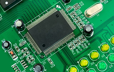
Parasitic capacitance is an unwanted and unavoidable phenomenon that causes electronic components to behave like capacitors due to their proximity.

Electronic components on a PCB
Capacitors store electric energy in an electric circuit. When two electrical conductors operating at different voltages are near each other, the electric field between them causes an electric charge to get stored between them. This charge-storage effect is called parasitic capacitance.
Types of Parasitics
There are three types of parasitics.
Parasitic Resistance
The Parasitic resistance can exist as a shunt between conductive elements or in series along traces.
Parasitic Inductance
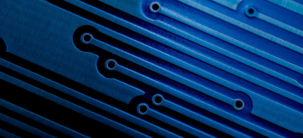
Parasitic inductance can exist along circuit board traces. It portrays similar characteristics to an actual inductor, which stores and dissipates electrical energy.

PCB traces
Parasitic Capacitance
As stated earlier, this phenomenon occurs when two conductive elements in proximity possess or are at different charge levels.
Difference Between Stray and Parasitic Capacitance
Some people use parasitic and stray capacitance interchangeably, but the two have different meanings. Stray capacitance explains the introduction of unwanted capacitance, while parasitic capacitance shows how the charge affects circuit operation.
Two adjacent conductors in a PCB can induce stray and parasitic capacitance. However, the effects of the surrounding environment can also cause stray capacitance.
Special Offer: Get $100 off your order!
Email [email protected] to get started!
What is the Parasitic Capacitance Effect?
Parasitic capacitance occurs between conductors, PCBAs, bare boards, and component packages (like SMDs). The two conductors or elements could be two traces, component pins, a pad & trace, pad & pin, or any other conductive elements on the PCB.
A potential difference causes an electric current to flow across intrinsic capacitor plates. However, as the stored charge increases, it reduces the potential difference, which slows the electron flow. Therefore, parasitic capacitance negatively impacts signal integrity by restricting current flow along the desired signal path.
An illustration of how capacitors store electrical energy
How Parasitic Capacitance Affects Electronic Circuits
Parasitic capacitance has little to no impact on low-frequency circuits. However, it is a matter of concern in high-frequency circuits because a capacitor's behavior changes as the frequency increases. Eventually, it shorts the high-frequency circuit.
In amplifier designs, parasitic capacitance between the input and output can create unwanted feedback. The normally open electrical signal path becomes conductive when operating at high frequencies, causing unwanted oscillation. Parasitic oscillation in the amplifier circuit is the unintended feedback between the input and output of electronic components.
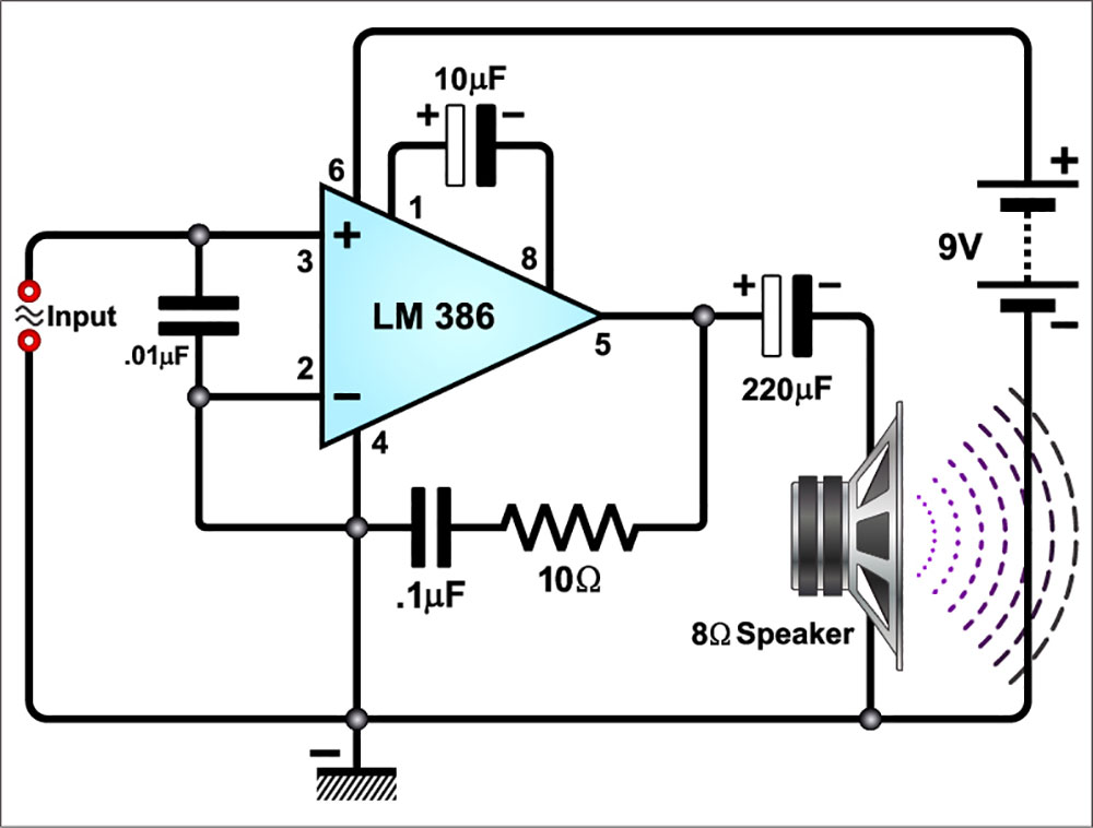
A simple audio amplifier circuit
The phenomenon is also troublesome between two adjacent components. If one of them propagates a high-frequency signal, it can cause crosstalk or EMI noise on the other conductor.
Besides causing interference, parasitic capacitance can affect the signal's integrity. For instance, if it builds up between a conductor and a ground plane, the elements can short at high frequency, altering the conductor's signal.
How To Reduce Parasitic Capacitance
It is impossible to eliminate parasitic capacitance. However, you can use the following strategies to reduce it in the PCB design and layout process.
Avoid Parallel Routing
Parallel routing creates a long stretch between two metals that develop maximum parasitic capacitance. Avoid this design strategy when doing the layout.
Parallel routing of PCB traces
Use Ground Planes Appropriately
An inner-layer ground plane has several benefits, such as improving heat dissipation while minimizing EMI and stray inductance. However, it can increase parasitic capacitance. Therefore, you should use it appropriately while weighing its pros and cons.
Moating
Power planes are AC grounds that behave similarly to ground planes. Therefore, removing or using them appropriately is vital for minimizing parasitic capacitance. Removing them from a conductor's vicinity is known as moating.
Reduce the Number of Vias
Vias are useful for connecting various layers in compact PCBs. However, using them excessively can increase parasitic capacitance significantly. Use them sparingly and avoid them on high-speed traces. Also, consider reducing annular rings around vias on layers with no connection to minimize the number of layers.

Via holes on a circuit board
Increase the Spacing Between Adjacent Circuit Board Traces
The capacitance decreases with distance. Therefore, you should create broader spaces between traces using the 2W or 3W rule. The wider clearance will also reduce cross-coupling.
Use a Guard Ring or Faraday Shield
A guard ring or Faraday shield operates as a shielding plate. Placing it between two traces will reduce parasitic capacitance significantly.
Impedance Matching
Multiple data lines transmit high data capacities per second, and they can cause impedance mismatch due to parasitic inductance and capacitance. Any parasitic-caused mismatch will produce reflections on the line that increase bit error rates and timing jitter. Therefore, ensure you match the impedance across the signal lines that transmit data at high speeds.
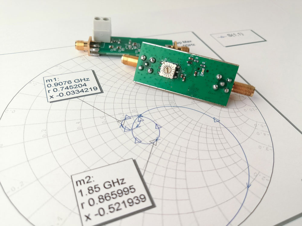
A radio frequency PCB on a Smith chart for impedance matching
Use the Correct Layer Thickness
While thin layers decrease the parasitic inductance and loop area, they increase the parasitic capacitance. Consider these factors to determine the best layer thickness. Try using simulation tools with multiple layer stacks for this task.
Separate Components Carefully
Careful separation of components and guard rings, wires, ground & power planes is essential for reducing parasitic capacitance. Also, implement shielding between the input and output and terminate the transmission lines properly.
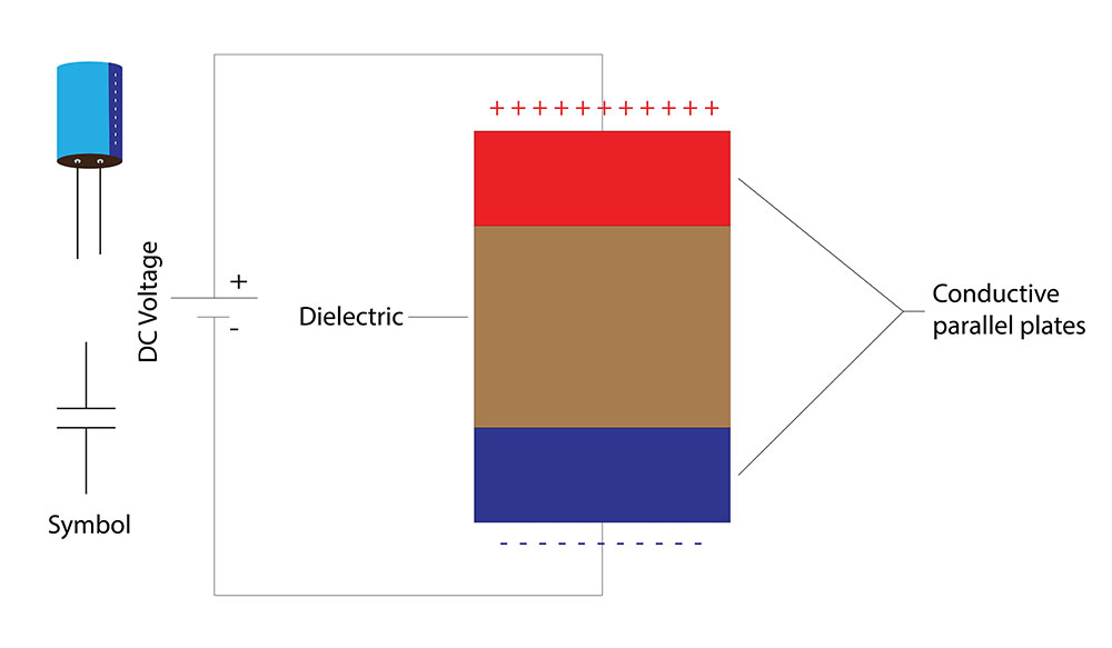
Use Low Permittivity Dielectric Materials
Dielectric materials with a high permittivity increase the stray capacitance. On the other hand, materials with low permittivity decrease the stray capacitance. However, this phenomenon assumes all other variables remain constant.
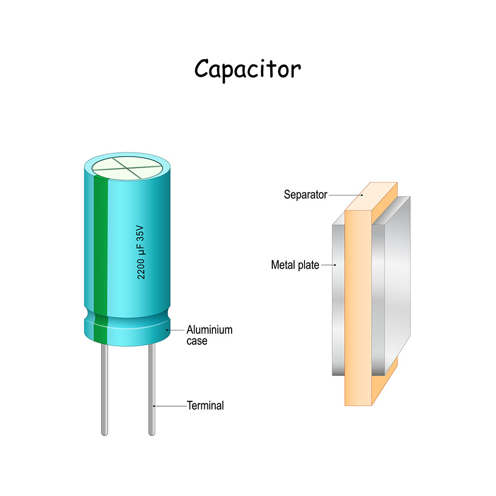
A dielectric material or separator. It sits between two conductors, such as traces on PCBs.
Sandwich the Signal Layer
If designing a 4-layer board, place the power plane on the lowest layer, then sandwich the signal layer between the power and ground plane. You can also route the sensitive traces between two ground planes. This design will keep EMI from signals in one layer from inducing noise in the transmission lines of the adjacent layer.
How To Calculate Parasitic Capacitance
Parasitic capacitance is the storage per unit change in electric potential and is an inherent property of the conductors. You can calculate this parameter using the following formula.
C=q/v
Where
- C = capacitance (farads)
- q = charge (coulombs)
- v = voltage
dv/dt=0 if the electrical signal is constant and does not change over time. This equation implies no potential change, and i=0. But if there is a capacitor in the loop, dv/dt will equate to a fixed value. This value means there is a potential change, which will cause an electric current to flow. Therefore, i≠0.
Calculating Trace Parasitic Capacitance
You can calculate the parallel plate capacitance using the following formula.
C = (kA/11.3d)pF
Where
- C = capacitance
- k = board material's relative dielectric constant
- A = plate area (cm2)
- d = distance between plates (cm)
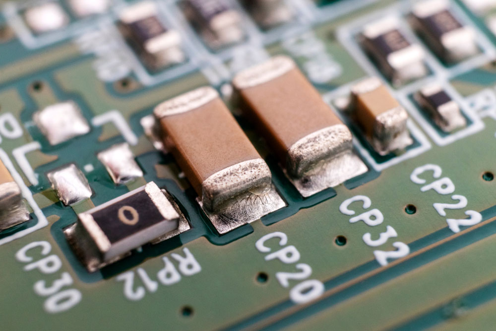
Surface-Mount capacitors on an LCD TV's circuit board
How To Measure Parasitic Capacitance Using a TDR
While it is possible to use a high-resolution LCR meter to measure parasitic capacitance, a Time Domain Reflectometer (TDR) is more accurate. Why? A TDR enables you to measure capacitance on devices and structures directly as they are on the circuit.
Surrounding environments can affect capacitance, so it is better to do measurements on different devices as they are on the circuit.
On top of that, TDRs allow individual measurements of the device and transmission line characteristics without removing any component from the circuit.
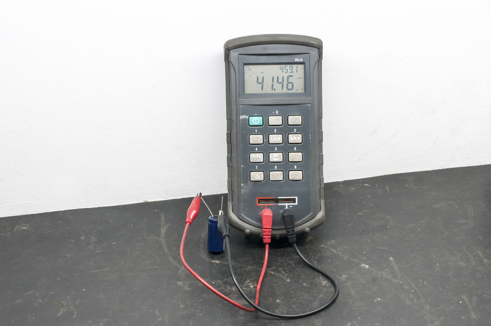
An LCR meter for measuring inductance (L), capacitance (C), and resistance (R)
Considering a board with long, narrow traces that form microstrips over a ground plane, the copper lines go from top to bottom through vias. If these vias form parasitic capacitance with the ground, you can propagate a step wave on the trace, then observe the reflected waveform from the via-hole discontinuity.
After that, calculate the 'excess' capacitance caused by the via by integrating and scaling the waveform. This calculation gives the accurate capacitance for the model.
Wrap Up
In conclusion, a non-zero capacitance will always exist between two conductors. However, it is possible to optimize the PCB layout to minimize the effect and enhance the circuit's performance & signal integrity. We hope this article has been insightful. If you have any questions or comments, drop a message, and we'll get back to you asap.
Special Offer: Get $100 off your order!
Email [email protected] to get started!