If you are looking for a single-layer PCB, you have come to the right place. This blog post will discuss everything you need about the single-sided board.
Moreover, we will talk about the benefits of using them, as well as some of the drawbacks.
By the end of this post, you should understand what single-layer PCBs are and whether or not they are the right choice for your project! Whether you're a PCB board manufacturer or a hobbyist, understanding these boards can greatly enhance your design choices.
Contents
- Single-Sided PCB-What is Single Layering?
- Construction of Single-Layer PCB
- single Layer PCB Stackup
- Single-Layer PCB Thickness
- Single Side PCB Raw Material
- Aluminum
- Fr4 Grade Fiberglass Laminates
- Cem 1
- Cem 3
- Copper base
- Differences Between Single-Layer and Multilayer PCBs
- Types of Single-Layer PCB
- -Single Layer Flexible PCBs
- -Single-layer rigid PCBs
- -Single Layer Rigid and Flexible PCB
- -Single Layer High-Frequency PCB
- -Single Layer Aluminum PCB
- Advantages of the single-sided circuit board
- Disadvantages of single-layer circuit board:
- Single Layer PCB Applications
- Single-layer PCB design
- Single-layer PCB design software
- How do I make a single-layer PCB?
- Single Layer Rigid PCBs Manufacturer
- How To Maintain a Single-Sided PCB
- Observation
- Testing
- Component Inspection
- Maintenance/Repairs
- Cost of Single-Layer PCB
- Summary
Single-Sided PCB-What is Single Layering?
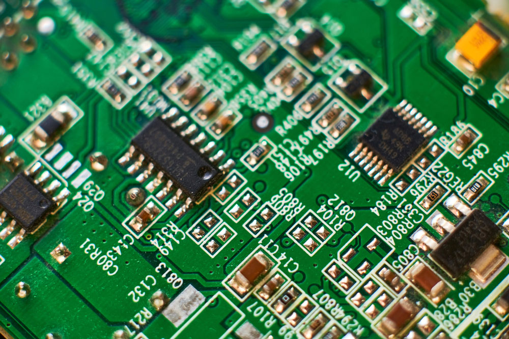
Circuit Boards close up with a short Depth Of Field, close up.
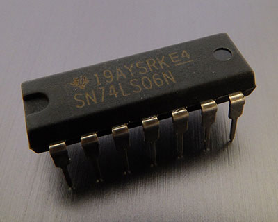
A single-sided PCB, or a single-layer PCB, is a circuit board with only one layer of conductive materials.
In addition, this layer is typically made of copper foil, and manufacturers etch them with the circuit pattern.
Also, the single-sided PCB is the most basic type of PCB, and it is applicable in various applications.
Construction of Single-Layer PCB
A single-layer PCB only has one conductive layer but needs a base or substrate material to provide structural support.
The type and nature of this substrate material determine the board’s applications and flexibility/rigidity.
On the conductive layer, the foil’s thickness can vary, depending on the application, and you can define it in ounces per square foot.
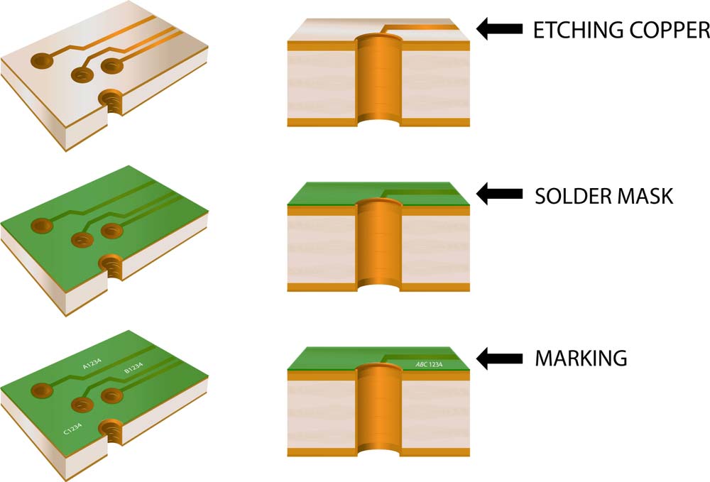
Copper, solder mask, and silkscreen layers on a PCB
The board also needs a solder mask layer above the copper traces to protect it from corrosion, shorting, and other faults.
The final layer in the stack is the silkscreen, which indicates the component characters, symbols, and values on the mounting surface to simplify the assembly process and understand the board operations better.
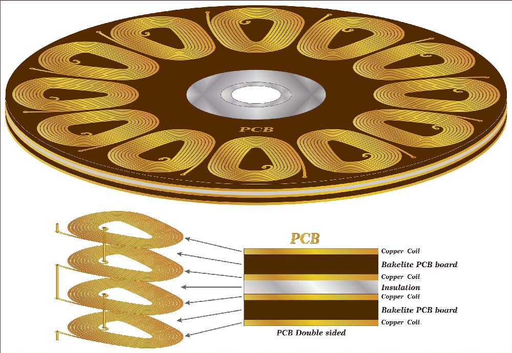
single Layer PCB Stackup

Single layer pcb stackup
As we can see from the picture above, a single-layer PCB has only one layer of conductive materials.
And this layer is for the circuitry. So, if you want to add more components to the PCB, you must put them on the other side of the board.
Single-Layer PCB Thickness
The industry standard for PCB thickness is about 1.57mm or 0.062 inches, but it can range from 0.2mm to 6.1mm depending on its construction.
Those on the lower end of the scale are usually flexible boards because the copper layer’s thickness is usually standard in single-layer boards.
These boards usually don’t have holes or thick copper traces to handle high-frequency signals.
Therefore, altering the thickness of the substrate layer can make the PCB rigid or flexible.
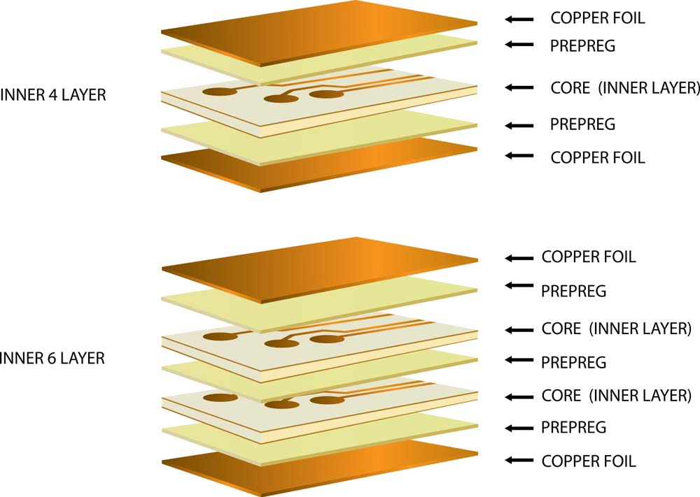
A 4-layer vs 6-layer PCB stack (note the increase in thickness)
Single Side PCB Raw Material
Multiplied printed circuit boards PCB isolated on a white background. PCB assembly.
Aluminum
Aluminum is the most common single-layer PCB raw material. An aluminum material substrate is also the cheapest one. The main advantage of aluminum is that it has good heat conduction. So it can dissipate heat quickly.
Fr4 Grade Fiberglass Laminates
FR-4 is a common dielectric used in single-side PCBs. FR stands for Flame Retardant, and it is made of fiberglass. The main advantage of FR- is that it has good heat resistance and is cheaper than other dielectrics.
Cem 1
CEM-1 is a low-cost single-layer PCB. Besides, It uses fiberglass and epoxy. The main advantage of CEM- is that it has good heat resistance and is cheaper than other dielectrics.
Cem 3
CEM-3’s main material is fiberglass and epoxy. Plus, it is a single-sided PCB with good heat resistance. The main advantage of CEM- is that it has good heat resistance and is cheaper than other dielectrics.
Copper base
A copper single-layer circuit board uses a thin layer of copper foil that gets laminated onto a dielectric substrate.
The main advantage of the copper single-layer circuit board is that it has excellent electrical and thermal conductivity.
Usually, copper single-layer PCBs are useful in high-power applications where heat dissipation is a concern.
Differences Between Single-Layer and Multilayer PCBs
The primary difference is in the number of conductive layers defining the two.
Single-layer PCBs have only one conductive copper layer on one side of the substrate.
But multilayer boards have three or more copper trace layers separated by the core and prepregs.
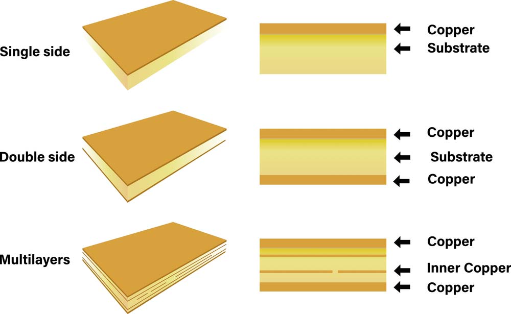
A single-layer PCB stack up compared to a double and multilayer board
This difference brings about other variations in their properties. For instance, the single copper foil layer only allows the board to accommodate a few components on one side of the board.
On the other hand, the multiple copper layers in multilayer PCBs enable them to accommodate denser component populations on either side of the board.
Plus, they can have structures like via-hole to interconnect the layers or evacuate heat. Single-layer PCBs don’t need vias.
But, designing multilayer boards is more challenging, especially if its function is to handle high-speed, high-frequency signals. Repairing them is also not a walk in the park.
On the bright side, their sophistication makes them ideal to use in multi-feature electronics in communication, aerospace, military, surveillance, and other demanding applications.
Single-layer boards can only provide enough circuitry for simple devices like LED flashlights and calculators.
A multilayered printed circuit board
Types of Single-Layer PCB
circuit Boards with chips and radio electronics components
In this section, we will talk about the single-layer circuit board in detail.
-Single Layer Flexible PCBs
Single layer pcb uses flexible material and is common in applications where you need to bend or flex the board. Plus, these types of pcb can be useful in high-temperature applications.
-Single-layer rigid PCBs
These are the most common types of single-sided PCBs. These types of boards are using of rigid material and are applicable in a variety of applications. Also, these boards can prevent crosstalk and are resistant to electromagnetic interference.
-Single Layer Rigid and Flexible PCB
Rigid-flex PCBs are single-layer boards that have both rigid and flexible sections. These boards are common in applications where the board needs to be bent or flexed. Plus, these types of pcb can be used in high-temperature applications.
-Single Layer High-Frequency PCB
High-frequency pcb are single-layer boards made with materials that can support high frequencies.
Teflon or polyphenylene oxide (PPO) is usually used to make the boards.
When selecting high-frequency single-layer PCBs, there are a few things to consider. Such as dielectric loss, thermal expansion, water absorption, etc.,
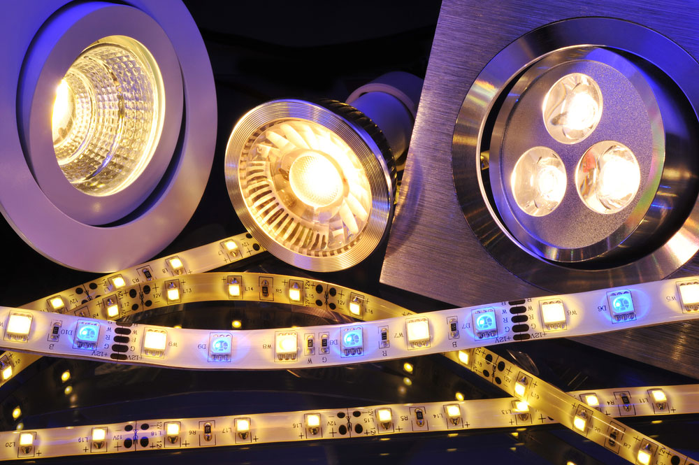
-Single Layer Aluminum PCB
Aluminum PCBs are single-layer boards that have an aluminum core.
They are common in high-power applications and have several advantages.
Aluminum PCB is more durable than other single-layer circuit boards and can dissipate heat more effectively. Moreover, they are also less likely to warp.
Special Offer: Get $100 off your order!
Email [email protected] to get started!
Advantages of the single-sided circuit board
Holding pcb chip assembly on pcb background on the production of PCBs
The single-sided PCB has several advantages:
-Firstly, it is the cheapest and easiest type of turnkey pcb manufacturing. Therefore, it is ideal for prototyping and small-scale production runs.
- Secondly, single-layer circuit boards are simpler to design than multi-layer PCBs. This is because there is only one layer of conductive material, simplifying the routing of tracks.
- Thirdly, single-layer circuit boards are more reliable than multi-layer PCBs. This is because there are fewer opportunities for errors to occur during the manufacturing process.
Single-layer circuit boards are the best choice for simple electronic projects. However, it would be best if you used a multi-layer medium to high volume pcbs for more complex projects.
-Fourthly, we will install various components on the single-layer circuit board. As a result, there will be a lower jumper to make up for the circuit.
-A single-layer circuit board is more flexible than a multi-layer PCB. This is because it can be bent without damaging the tracks.
-Plus, the single pcb reduces manufacturing, assembly, and material costs. Therefore, you will lower the cost of overall pcb.
-And the lead time is short, better for mass production. Suitable for low to medium-volume production runs
-Finally, single-layer PCBs are more cost-effective than multi-layer PCBs. This is because they require less material and labor to produce.
Disadvantages of single-layer circuit board:
- - Limited to low pin count devices or simple devices
- - More susceptible to electromagnetic interference
- - Not suitable for high-speed or high-density circuits
- It is more difficult to route complex circuits.
- Limited to one side of the board, unlike double-sided pcb or multi-layer PCBs.
Single Layer PCB Applications
Printed circuit board (PCB) on white background
Where are single-layer PCBs used? The following are some of the single-layer pcb uses.
Single-sided pcb boards are most commonly applicable in low-density applications, such as:
- Resistors
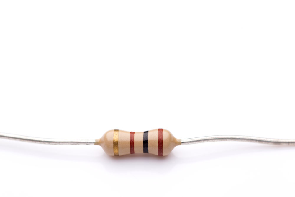
Electrical resistor isolated on a white background. Electric circuit component
- Diodes
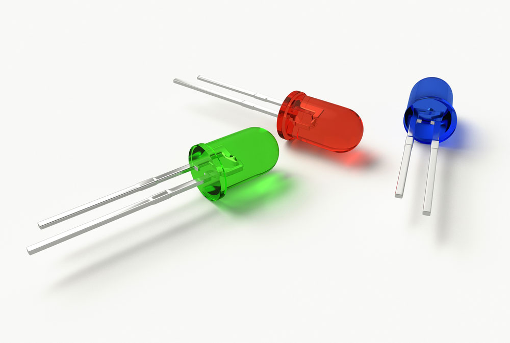
3 mm LED, RGB (red, green, blue)
- Capacitors
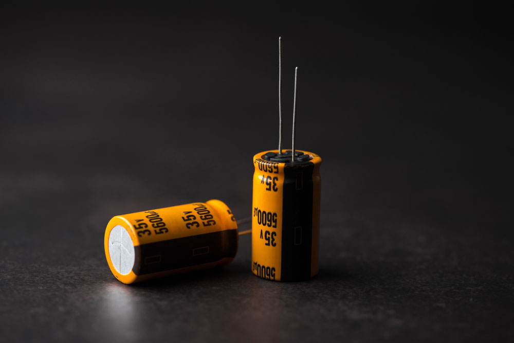
Isolated capacitor, used in the electronic device.
- Inductors
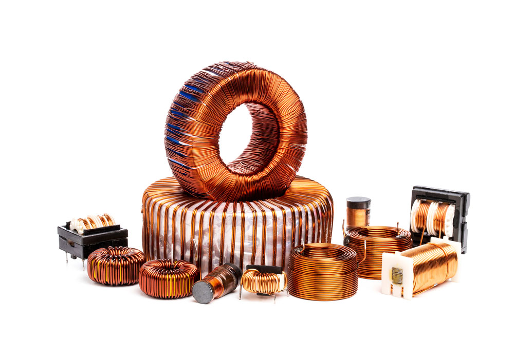
Set of electric copper coil inductor isolated on white background
- LEADS
different current LEDs-technologies in one picture
- Switches

Turning on or off on light switch with wood wall at home.
-Coffee makers

Woman making fresh espresso in the coffee maker.
-machine circuits
-power supplies
-timing circuits
These single-layer pcb applications are suitable for boards that have less wiring. Also, single-layer pcb is applicable because they are easy to design, and the manufacturing process is simpler than multilayer pcb.
Single-layer PCB design

Female Electrical Engineer Works on Computer with CAD Software.
The single-layer board design is the process of designing printed circuit boards with only one conductive layer. Here are some tips for single-layer circuit board design.
- - Keep the design as simple as possible.
- - Use wide traces for power and ground lines.
- - Use vias sparingly.
- - Keep the board as small as possible.
- - Use a ground plane if possible.
- - Keep trace lengths as short as possible.
- - Avoid using buried or blind vias.
If you need help with single-layer design, contact an experienced PCB designer. They can help you navigate the challenges of single-layer circuit design and ensure that your board is manufactured to the highest quality standards.
Single-layer PCB design software
1 layer PCB's design software is a great tool for designing single-layer PCBs. This type of software allows you to design your board using various tools and features. You can also use single-layer PCB design software to create multiple versions of your board to test and iterate on your design until it is perfect.
There are a few things to remember when using single-layer PCB design software.
First, make sure that you select the right tool for your needs. Many types of single-board design software are available, and not all will be right for every project.
Second, take the time to learn how to use the software. While most design software is fairly easy to use, it is still important to take the time to learn how to use it properly.
Finally, make sure that you test your design before you commit to using it. This will ensure that you are happy with your final product.
How do I make a single-layer PCB?
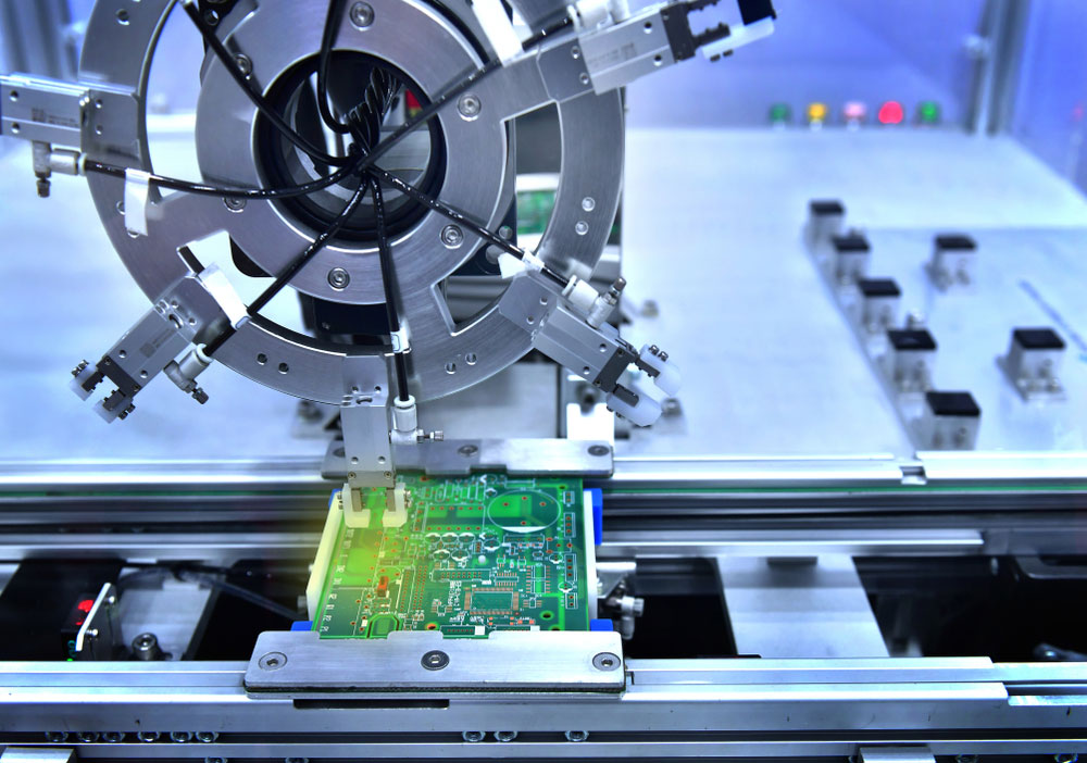
The technological manufacturing process of de-soldering and assembling components on circuit boards.
Making a single-layer PCB is not as complicated as it may seem. You can use software like Eagle to design your single-layer pcb.
Once you have designed your board, you must send the design to a manufacturer who will produce the board for you.
The base material for a single-layer PCB is typically FR-42. This material is strong and heat resistant, making it ideal for single-layer pcb applications.
In addition, base material types and the nature of the dielectric layer are also single-sided pcb factors that will affect your choice of single-layer pcb.
Other factors that you should consider when choosing a single-layer pcb include the thickness of the copper, the number of layers, and the board size.
You can also choose to have your single-layer pcb made with a lead-free finish.
Single Layer Rigid PCBs Manufacturer
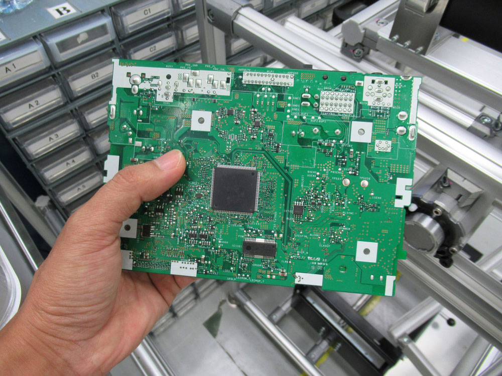
Electronics Manufacturing Services, Assembly Of Circuit Board arrangement, close-up of the raw PCBA in the tray.
Once you have decided on the specifications for your single-layer PCs, you must find a manufacturer to produce the board for you.
- Many manufacturers offer single-layer circuit board services, so be sure to research each one carefully before making your decision.
- It would be best to ask for quotes from multiple manufacturers before making your final choice.
- Single pcb can be a great option for various applications, so consider all the factors mentioned above before making your final decision.
How To Maintain a Single-Sided PCB
Observation
The first step involves optics. Check the board to understand its connection interfaces and components mounted on the board.
Testing
Do a preliminary inspection to try to find the faulty area using a multimeter. You might have to test different components when troubleshooting the issue before you locate the culprit.
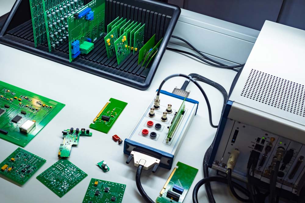
PCBs undergoing testing for quality control
Component Inspection
After identifying the fault, you might have to remove some components. You’ll need a soldering iron.
Maintenance/Repairs
Replace the components and transmission lines if faulty. After that, test the PCB, then return it to service when it passes. Otherwise, you’ll have to re-test or replace the board.
Cost of Single-Layer PCB
Since it has the simplest structure, the cost of a single-layer circuit board is the lowest compared to double-sided and multilayer PCBs. It can even cost you less than a dollar.
However, the cost can vary depending on the base material, board size, surface finish, and order volume. The higher the number of orders, the lower the cost per piece.
So, the best way to know the cost of a single-layer PCB is to contact your PCB fab house, send them your requirements, and request a quote.
Summary
A single-layer circuit board has one copper layer used to create the circuits on the board.
Single-layer boards are less expensive than other types of PCBs because they are simpler to manufacture.
They are also smaller and lighter than other types of PCBs, making them ideal for small devices such as cell phones and portable electronics.
A single-layer board may be the perfect solution if you need small, lightweight, and inexpensive PCBs for your project.
While there are some concerns that need to be addressed, the potential benefits of single-sided boards warrant further exploration.
With continued research and development, these boards could become a viable solution for smaller devices and help reduce costs and environmental impact.
Have you tried using a single circuit board in your project? Let us know how it went in the comments below.
Special Offer: Get $100 off your order!
Email [email protected] to get started!