Contents
- Transparent PCB vs. PCB: Comparing Transparent PCB to Traditional PCBs
- Transparent PCB Substrate
- The Base Materials of Transparent PCBs
- Clear PCB: Transparent Glass PCB
- Benefits of Transparent Glass PCBs
- Clear PCB: Ceramic Transparent Circuit Boards
- Advantages of Ceramic Transparent Circuit Boards
- Applications of Transparent Ceramic Circuit Boards
- Clear PCB: Transparent Flexible PCBs
- Advantages of Transparent Flexible PCBs
- Transparent Flexible PCB Applications
- How to Make a PCB Transparent?
- Design Rules for Transparent Circuit Boards
- Limitations and Challenges of Transparent PCBs
- Lower Fabrication Yield
- Higher Manufacturing Cost
- Higher Chances of Warping
- Laser Drilling Limitations
- Low Component Density
- Thermal Management
- Conductor Oxidation
- Complex Assembly Process
- Difficult to Repair
- Safety Standards
- Signal Quality
- DC Resistance
- Environmental Benefits of Transparent PCBs
- They Require Eco-Friendly Materials
- They Are Easier To Recycle
- They Reduce Waste During Manufacturing
- They Have a Smaller Carbon Footprint
- They Have a Lower Power Consumption Rating
- Future Trends in Transparent PCBs
- Manufacturing Improvements
- New Transparent Substrate Materials
- Additive Processing
- Touch Integration and Miniaturization
- Design Automation
- Transparent PCB by OurPCB
Transparent PCB vs. PCB: Comparing Transparent PCB to Traditional PCBs
Transparent printed circuit boards feature see-through base or substrate materials that allow light to pass through to the other side. These materials include polycarbonate, ceramic (aluminum oxide, magnesium oxide, alumina, etc.), PET (polyethylene terephthalate), glass-reinforced epoxy, liquid crystal polymer, and PMMA (polymethyl methacrylate).
However, traditional PCBs have opaque substrates that are usually fiberglass-based materials like FR4. Some can even have metal substrates like aluminum or even opaque ceramic.
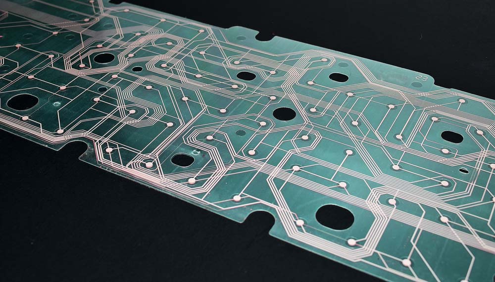
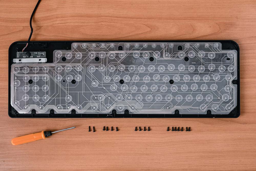
A transparent, flexible keyboard PCB
Transparent PCB Substrate
As stated above, transparent PCBs can have a glass or ceramic substrate. Ceramic material transparent substrates have a higher thermal conductivity than their glass counterparts. However, glass PCB substrates offer better optical transmissivity than the ceramic type. The optical transmissivity of glass PCB substrates is about 99.5-99%, while that of ceramic ranges from 75-80%.
The Base Materials of Transparent PCBs
Transparent PCBs can be rigid or flexible. For instance, the rigid ceramic PCBs contain an aluminum substrate, usually in the form of the following:
- Aluminum oxide
- An amalgam of magnesium and aluminum
- Magnesium oxide
- and more
These materials assure roughly 80% transparency. Also, an oily, water-based nano-blue phase alumina enhances the hardness of the resin materials from 6H to 8H.
However, the base materials in the flexible type of transparent PCBs are polyimide and polyester. These have almost 95% transparency.
Flexibility does not mean the boards are weak. On the contrary, the Polyimide-based PCB types are strong enough to handle mechanical and electrical stresses. Additionally, they are resistant to thermal pressure.
Clear PCB: Transparent Glass PCB
Glass is a material made using a mix of soda, limestone, ash, and sand. Additionally, these materials are abundant in nature and easily recyclable. Therefore, glass is an eco-friendly material.
However, regular glass is not very sturdy, so you will most likely see tempered glass. Tempered glass is a reprocessed and prestressed glass to maximize durability. Besides, it has better shock and impact absorbing capabilities, making it useful for extreme applications.
But tempered glass isn't the sturdiest glass variety. Sapphire glass is the strongest and most durable of them all. Therefore, it is the go-to glass PCB material for high-end electronics and space/satellite devices because of its thermal properties and high dielectrics.
In addition, glass transparent PCBs have a 360° luminescence. Therefore, light can flow out in all directions.
Benefits of Transparent Glass PCBs
- Extremely flat (ideal for symmetrical functionality)
- High heat resistance
- Resistant to deformation
- Highly resistant to wear and tear
- Cheap, recyclable raw materials
- Highly transparent
Clear PCB: Ceramic Transparent Circuit Boards
PCB manufacturers usually make transparent ceramic circuit boards using materials like aluminum oxide, alumina, magnesium oxide, al-mg spinel, etc. These boards have a transparent substrate and a glass-based solder mask to help maintain the substrate's transparency at 75-85%. However, their conductors and conductive traces are not transparent.
Advantages of Ceramic Transparent Circuit Boards
- High thermal conductivity (24-31.4 W/mK) - To explore more about these high-temperature materials, visit high-temperature PCBs.
- Low and stable thermal expansion coefficient
- Highly temperature resistant (over 2000°C)
- No water absorption with superb electrical insulation
- Multiple optical features
Applications of Transparent Ceramic Circuit Boards
- High power LED PCBs
- Optical sensors
- Aircraft and missile infrared windows
- High-pressure sodium lamps
Special Offer: Get $100 off your order!
Email sales@ourpcb.net to get started!
Clear PCB: Transparent Flexible PCBs
Transparent flexible circuit boards contain PET thin films that are either light blue, white, transparent, light green, or other colors. However, the pads and copper traces in these PCBs are not see-through.
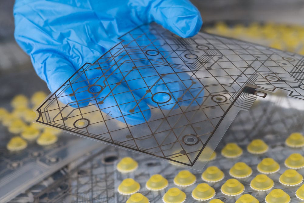
A transparent flexible PCB
But there is a variant that has transparent copper traces. So, making these boards requires a unique technique that involves clamping the circuit between two PET films.
Advantages of Transparent Flexible PCBs
- Provides multiple optical features
- Bends, twists, folds, and moves arbitrarily in 3D space
- 90% lighter than rigid PCBs
- Nano/micro level accurateness in PCB manufacturing
- Ideal for miniaturization, thinning and reducing product weight
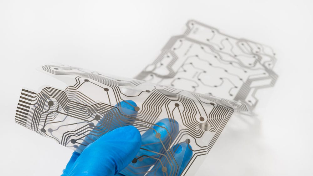
A clear, flexible PCB with copper traces
Transparent Flexible PCB Applications
- ABS systems
- Automatic control
- Mobile phones
- Cameras
- Instrument panels
- Medical devices
- Smart contact lenses
- Electronic skins
How to Make a PCB Transparent?
Since it is unlike the conventional circuit board, you need to use the following steps to make a PCB transparent.
- First, arrange the required materials (copper foil, ferric chloride, polyester, etc.).
- Second, prepare the circuit design layout and print it.
- Third, fabricate the substrate using transparent materials.
- Fourthly, add copper foil and apply the photoresist.
- Next, expose the setup to sunlight or an artificial light source.
- Then, develop the photoresist.
- After that, etch the board using a ferric chloride solution to eliminate the unwanted copper.
- Finally, wash and dry the PCB.
Design Rules for Transparent Circuit Boards
Transparent PCBs require the following critical design rules to optimize their performance.
- First, a high volume transparent flexible PCB should have a panel dimension of over 100mm (for PCBs having more than 50 panels)
- Secondly, the ideal board thickness is 0.38mm
- Metallization should be a silver-palladium alloy
- A panelized transparent board should have a five and one-ounce conductor thickness
- Immersion gold and ENIG are the best surface finishes for these PCBs
- The standard solder resist minimum opening should be 0.2mm
- 5-12 mils via diameter
- 3-12 mils minimum via spacing
- Short and direct trace length
- Include a power plane for smooth ground and power plane distribution
- Also, keep the board components and related test points together
- Less than 4mm dimensional tolerance
- 10% and 4 mils thickness and hole tolerances, respectively
- Less than 0.5 micrometers of surface roughness
- 0.8 mils minimum line spacing
- Use decoupling capacitors to minimize noise in high-speed signal transmission and explore EMI design strategies for transparent PCBs.
- Design rules might change, so check regularly
Limitations and Challenges of Transparent PCBs
Although they are more visually appealing than traditional opaque PCBs, transparent circuit boards have some challenges and limitations in performance and fabrication.
Lower Fabrication Yield
Manufacturing these circuit boards requires specialized processing steps that make it more challenging to come up with operational custom printed circuit boards at the end of the production line.
Higher Manufacturing Cost
In addition to having a lower manufacturing yield, fabricating transparent PCBs is costly because the materials cost more than the fiberglass materials for standard boards.
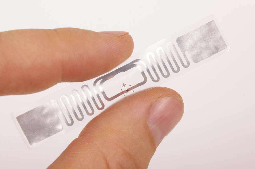
A transparent, flexible RFID transponder PCB with an antenna
Higher Chances of Warping
Transparent PCB materials can warp more easily than fiberglass because they are not solid.
Working on these surfaces can be tricky and cause high losses that lower the fabrication yield.
Laser Drilling Limitations
Projecting a laser beam on the thin transparent PCB can crack the substrate, especially if the drill is boring a big hole.
Therefore, you are limited in terms of the hole size you can drill and the number of holes you can create.
Low Component Density
Although transparent PCBs are see-through, components and copper traces are not.
So, the more components and copper layers you have, the less transparent the board will be.
High-performance PCBs usually have four copper layers at most to maintain transparency.
Thermal Management
Unlike opaque PCBs, you cannot have heat sinks or multiple thermal vias to evacuate heat from the components or transmission lines. So, you must incorporate efficient thermal management in the design phase.
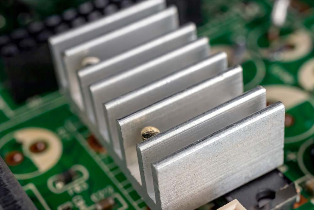
An aluminum heat sink on a PCB
Conductor Oxidation
Although the goal is to have the transparent PCB as thin as possible, you must incorporate a coating layer above the outer copper lines to protect them from oxidizing.
Complex Assembly Process
Soldering components on these circuit boards is a tricky affair because you have to maintain transparency.
Also, high heat levels during reflow soldering can damage the substrate. That’s why partnering with PCB assembly design services is essential to ensure expert handling and precise soldering of components on these boards.
Difficult to Repair
These boards are equally as challenging to troubleshoot and repair, especially if the process requires reworking.
Safety Standards
Transparent PCBs are usually designed and manufactured for specific specialized applications, so they must meet some health, safety, or appliance quality standards to be approved for the market.
Meeting these standards requires meticulous planning and manufacturing, which is costly.
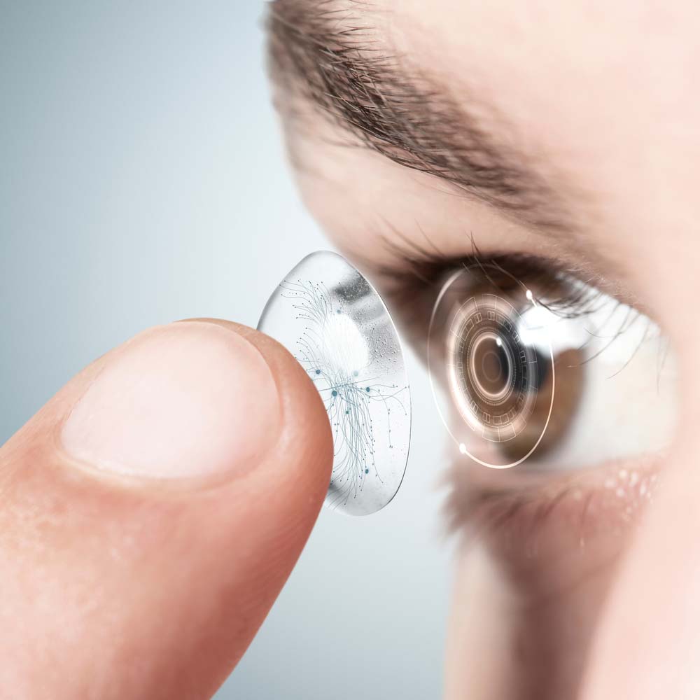
A smart contact lens with a transparent PCB
Signal Quality
If the board is meant for high-frequency applications, you must design the traces to handle these signals without degradation or attenuation. For optimal performance in such applications, consider using high-frequency PCBs, which are specifically designed to maintain signal integrity. Achieving this performance on a transparent PCB is no mean feat.
DC Resistance
A board’s DC resistance is determined by its trace conductivity and the cross-sectional area of the transmission lines.
Because the traces in transparent PCBs are thin, they experience higher DC resistance, which negatively impacts the conductors.
Environmental Benefits of Transparent PCBs
Not only are transparent PCBs visually appealing, but they are also good for the environment in the following ways.
They Require Eco-Friendly Materials
The materials used to make transparent PCBs, like soda-lime glass and ceramics, are eco-friendly, which means they are less harmful to the environment than fiberglass substrates.
They Are Easier To Recycle
In addition to being friendlier to the environment, transparent PCB materials are easier to recycle when the board reaches its end of life. Learn more about the recycling process and its advantages by visiting Recycling PCBs.
A transparent keyboard PCB(picture it with a transparent case)
They Reduce Waste During Manufacturing
Emerging additive manufacturing solutions used in transparent PCB fabrication reduce material wastage more than the subtractive methods used in traditional PCBs.
They Have a Smaller Carbon Footprint
Since they are thinner and lighter, transparent PCBs result in lower CO2 emissions during manufacturing and transportation.
They Have a Lower Power Consumption Rating
These see-through boards enable devices like edge-lit displays to consume far less energy than lighting and display devices bearing traditional opaque boards.
Future Trends in Transparent PCBs
The transparent PCB industry has improved tremendously since its inception. Some of the key areas and emerging trends that are shaping this circuit board industry include the following.
Manufacturing Improvements
Innovations in transparent PCB fabrication should increase yields, lower production costs, produce boards with better thermal management, more copper layers, via-holes, etc. The component density should also increase as the conductive layers increase.
New Transparent Substrate Materials
Manufacturers currently have limited transparent substrate materials, but these should increase in the future. Think of materials like hybrid polymers, nanomaterials, and conductive ink for the conductors.
Additive Processing
Additive fabrication is less wasteful, especially when creating transmission lines. This technology should become better with time, leveraging factors like inkjet printing to create electrical conductors.
Touch Integration and Miniaturization
Picture having a transparent smartphone. This is possible if manufacturers can integrate several features like touch into the transparent PCB. You can expect these boards to also be thinner for use in more compact electronics.
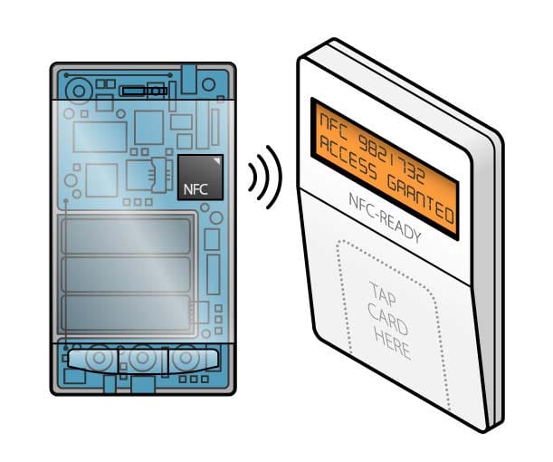
A transparent smartphone with an NFC chip for access control
Design Automation
Designers currently use CAD tools to make these circuit boards, but emerging AI technologies can automate and optimize the transparent PCB layout process.
All you have to do is give the software instructions and let it do the heavy lifting.
Transparent PCB by OurPCB
As the demand for innovative electronic devices grows, the need for specialised PCBs, such as transparent circuit boards, becomes increasingly important. OurPCB offers expert PCB manufacturing services tailored to meet these unique requirements. With a focus on quality and precision, we can help you create transparent PCBs that enhance the functionality and aesthetics of your projects. If you need Transparent PCB for your project, contact us for more details.
Special Offer: Get $100 off your order!
Email sales@ourpcb.net to get started!