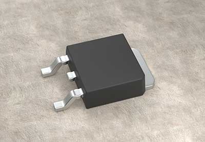
Over the years, multilayer printed circuit boards (PCBs) have grown in popularity across various industries. As a result, it has become increasingly easy to find different types of multilayer PCBs, including the 6-layer PCB.
6-layer PCBs have come to be an integral part of communication equipment and compact-sized wearable devices, but what makes them so important? This article aims to answer everything you need to know about 6-layer PCBs.
Contents
- What is a 6-Layer PCB?
- What are the Advantages of 6-Layer PCBs?
- Improved Signal Integrity
- Enhanced Durability and Reliability
- Increased Design Flexibility
- Better Power Distribution
- Cost-Effective for Complex Circuits
- What are the Layers in a 6-Layer PCB?
- How is a 6-Layer PCB Manufactured?
- Design
- Inner Layer Fabrication
- Layer Bonding and Lamination
- Drilling
- Plating
- Outer Layer Imaging and Etching
- Solder Mask and Silkscreen
- Electrical Testing and Inspection
- 6-Layer PCB Designs
- Stackup Considerations
- Material Selection
- Design for Manufacturing (DFM)
- Applications of 6-Layer PCBs
- High-Speed Digital Applications
- Compact Electronic Devices
- Communication Equipment
- Challenges in Designing 6-Layer PCBs
- Thermal Management
- Signal Integrity
- Cost vs. Complexity
- Comparison with Other Layer Counts
- 8-Layer vs. 6-Layer vs. 4-Layer PCBs
- 6-Layer PCB FAQs
- How is Power Routed on a 6-Layer PCB?
- When would you Need a 6-Layer PCB instead of a 4-Layer PCB?
- Can a 6-layer PCB be Repaired When Damaged?
What is a 6-Layer PCB?
A 6-layer PCB is a multilayer circuit board with six layers of conductive material separated by insulating layers. It can also be thought of as a typical 4-layer PCB with two additional signal layers.
The structure of the layers has different combinations of power planes, ground planes, and signal layers. This stacking method provides the main advantage of significantly reducing electromagnetic interference (EMI).
What are the Advantages of 6-Layer PCBs?
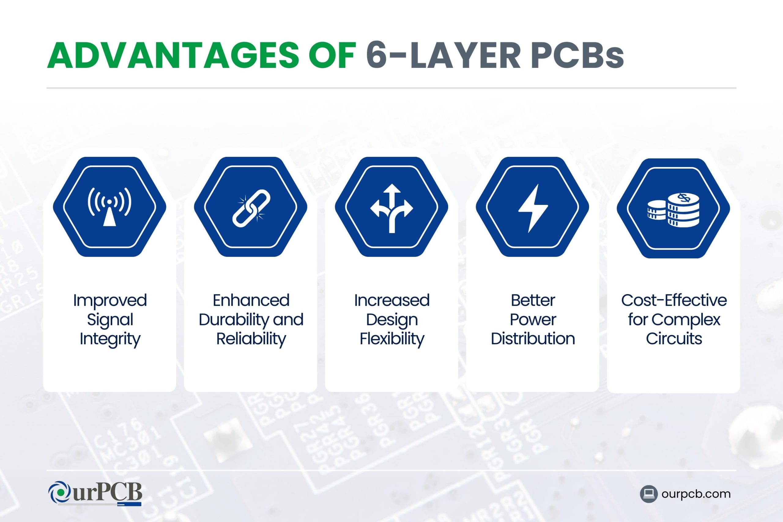
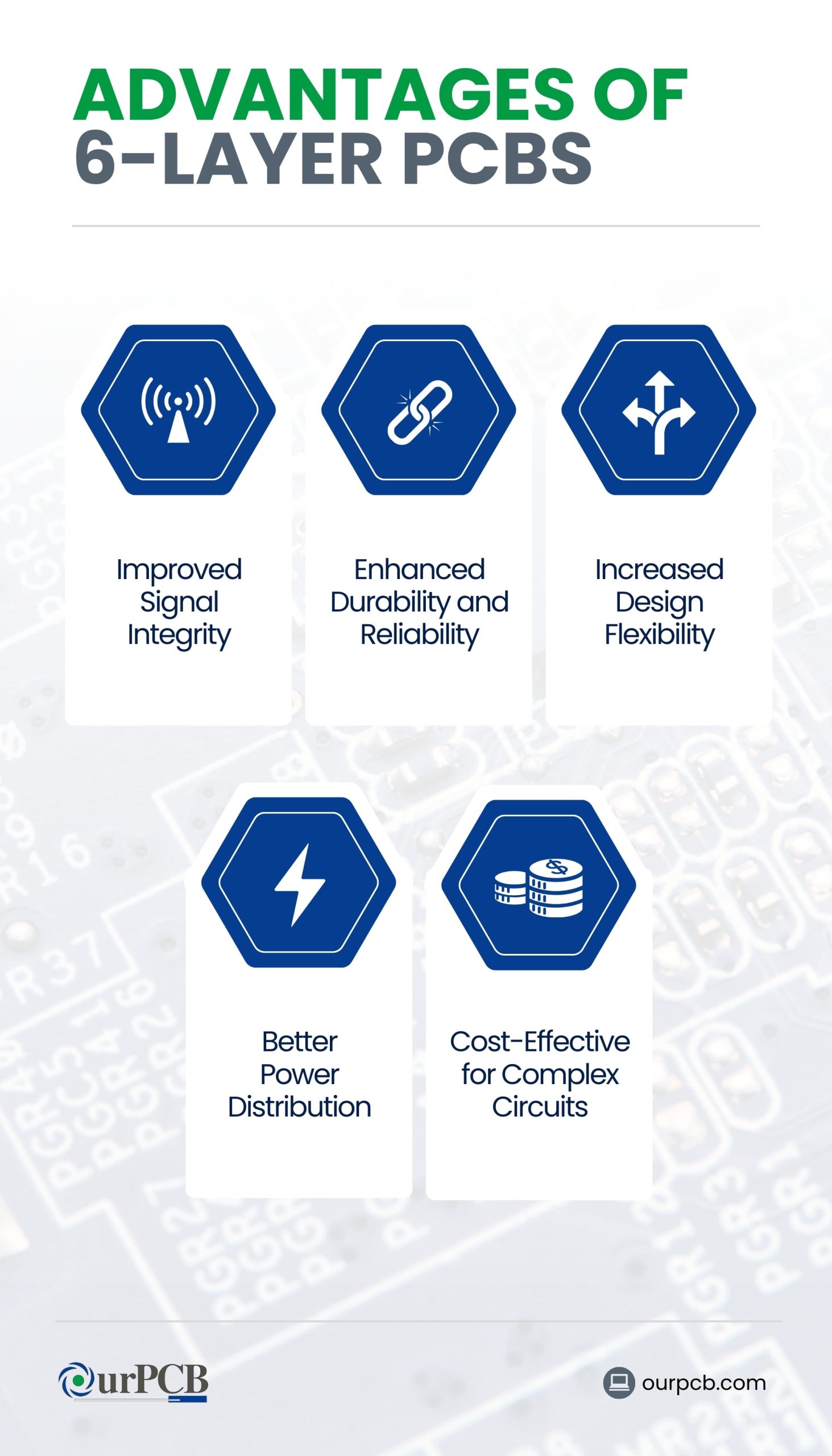
Improved Signal Integrity
A 6-layer PCB has extra layers that allow for better separation of signal traces, which reduces the risk of crosstalk. This is important in high-speed circuits, where interference can lead to data errors.
It also has controlled impedance routing because the signal layers are adjacent to ground planes, which further enhances signal integrity. Additionally, this helps maintain the signal waveforms.
Enhanced Durability and Reliability
Internal layers protect the signal traces from physical damage, like scratches, during handling or PCB assembly. Multiple layers within the PCB also provide protection from environmental factors like contamination and humidity, which can affect exposed traces.
The overall structural integrity of the PCB is higher than that of lower-layer PCBs, which makes it more reliable in high-stress applications like the automotive or aerospace industries.
Increased Design Flexibility
The six layers offer extra routing channels, which allows us to create more complex and densely packed circuits. This is useful in applications like field-programmable gate arrays (FPGAs) with many connections and microprocessors. There are many layers of stackup designs to optimize signal routing and isolation, which designers can tailor accordingly.
Better Power Distribution
Dedicated internal planes for power and ground drive a low-impedance path for better power distribution. This reduces noise and voltage drops, ensuring that all components receive equal and consistent amounts of energy. Moreover, the proximity of power and ground prevents energy from transferring from one part to another, which also helps with voltage and noise.
Cost-Effective for Complex Circuits
For complex circuits, multiple PCBs would be necessary if single or two-layer boards are used. In contrast, 6-layer PCBs are more cost-effective because they reduce material and assembly costs. In this way, they make the manufacturing process easier and improve performance and reliability.
Combining all these benefits into one PCB reduces the need for cables, connectors, and other testing, which leads to weight and space savings. Overall, assembly time is also saved, making the 6-layer PCB the premium choice for complex electronics.
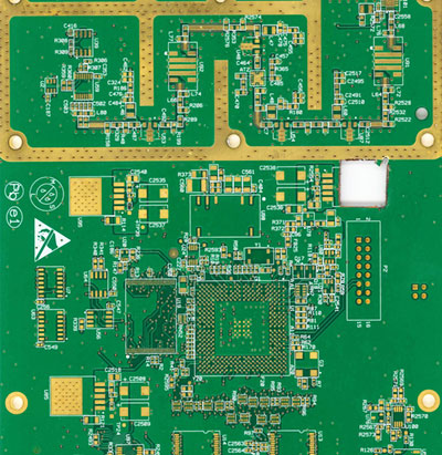
What are the Layers in a 6-Layer PCB?
A 6-layer board typically consists of the following layers, arranged in a specific order to enhance performance, signal integrity, and power supply:
- Top Layer (Signal Layer): This is the outermost layer on the top side of the PCB, which is used for routing signals and installing surface-mount components.
- Ground Plane: Aka, ground layer, this layer provides a low-impedance path for grounding and reducing EMI.
- Internal Signal Layer 1: This is for routing extra signal traces. It helps to manage complex routing and maintain signal integrity.
- Internal Power Plane: Used for power distribution (VCC), ensuring the stable supply of power to the components. This layer helps reduce noise and voltage drops.
- Internal Signal Layer 2: Another signal routing layer, used to manage complex circuits and reduce congestion on the other signal layers.
- Bottom Layer (Signal): This is the last layer on the bottom of the PCB. It is used for placing surface-mount components and routing signals.
Special Offer: Get $100 off your order!
Email [email protected] to get started!
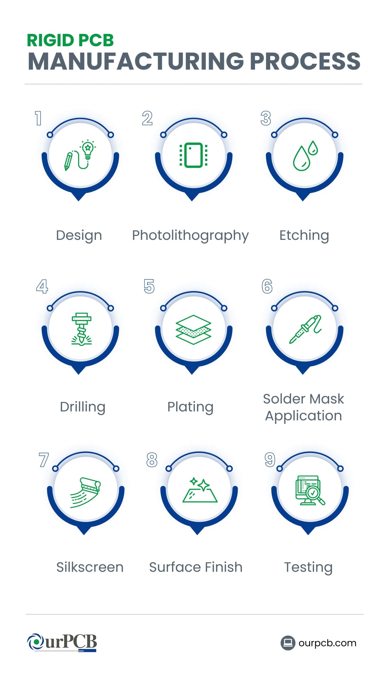
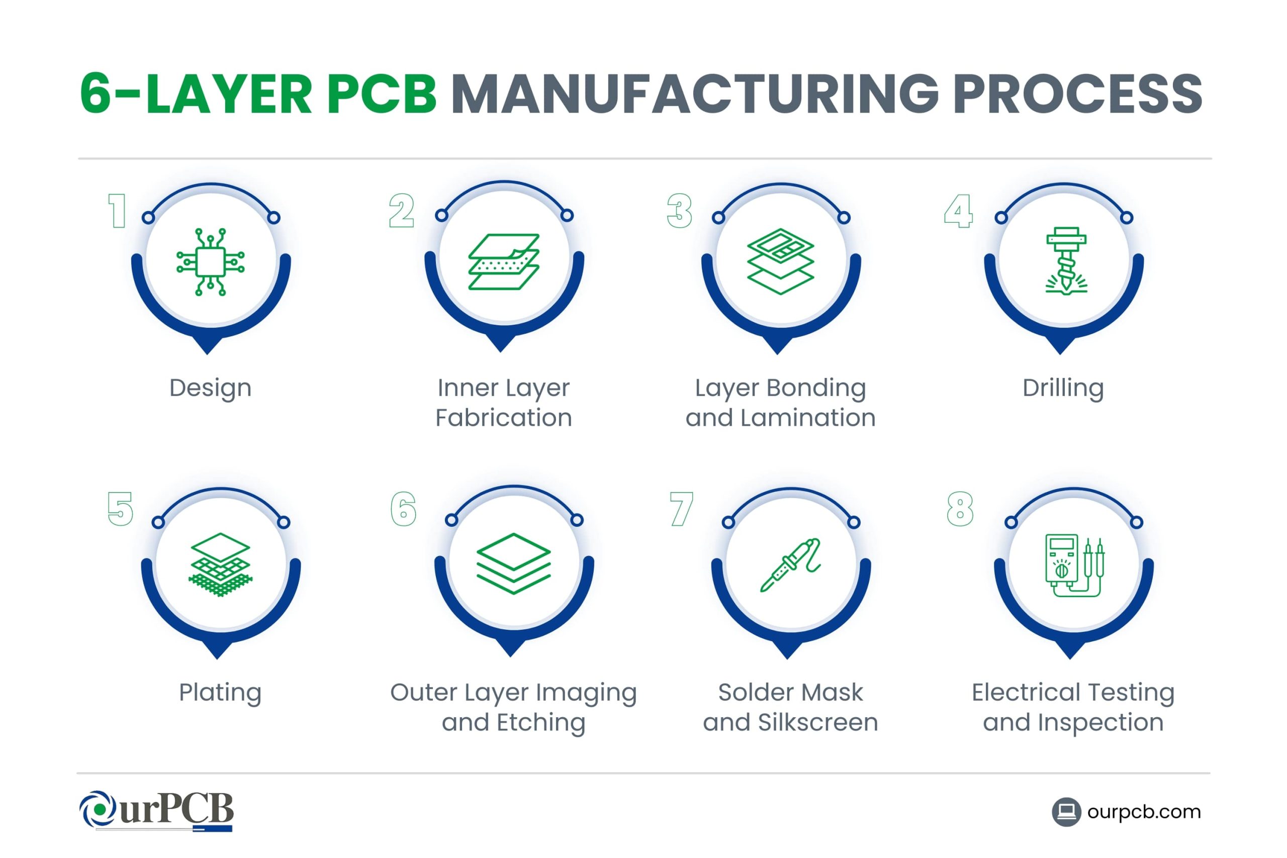
How is a 6-Layer PCB Manufactured?
-
Design
Schematic Capture
This is the first step in PCB design, where designers use Electronic Design Automation (EDA) software to create the electronic circuit. This software helps us map out the electronic components and connections, which is the blueprint for the PCB.
Popular EDA tools like Eagle, KiCad, and Altruim Designer have features such as netlist generation, electrical rule checking, and component libraries. These tools help streamline the design process by giving a visual representation of the circuit, which helps the user see that all connections are accurate before going to the layout phase.
PCB Layout
Using the EDA software, designers arrange components and traces on the PCB according to the schematic above. The layout process involves placing components correctly and routing electrical paths between them.
Following the planned PCB stackup is important, as it determines the arrangement of layers and routing of the ground path, power, and signal. This ensures that there is a high-quality signal and reduces interference. 3D PCB views and layer stackup diagrams can show the complexity of the process and highlight critical design points.
Manufacturing File Generation
After the PCB layout, the next step is to generate Gerber files (and others) to send the fabrication house. These files have detailed information about each layer of the PCB, such as drill holes, silkscreen patterns, solder masks, and copper traces. These files help to create the PCB in the most accurate manner possible.
-
Inner Layer Fabrication
Copper-Clad Laminate
The foundation of PCB manufacturing starts with copper-clad laminates, where the copper foil is laminated to insulating prepreg materials. These materials are the essential building blocks of the PCB’s inner layers and give the board thermal resistance and insulation constants, which all support proper performance.
Imaging
In this step, designers apply photoresist (resist) onto the copper layers and then direct UV light through a design pattern mask. This defines where the copper will remain, which ensures an exact circuit pattern. Likewise, this keeps the integrity of the circuit design.
Etching
This chemical process removes the exposed copper from the design mask, leaving the required traces and pads. Etching chemicals are very strong, and designers must handle them carefully to prevent harm and contamination.
Inspection
Automated optical inspection (AOI) is an automated visual inspection tool that checks that the etching process has accurately replicated the design. This is an important step, as it will catch defects earlier on and deliver high-quality inner layers.
-
Layer Bonding and Lamination
Prepreg Layup
This is where the inner layers will be layered with prepreg sheets and outer copper foils in preparation for lamination. The arrangement of these layers affects the PCB’s electrical properties and structural integrity,
Lamination
When the layers are put together, designers fuse them using specific temperature and pressure levels. This ensures that there is a solid, uniform bond without damage to the layers.
-
Drilling
CNC Drilling
Computer numerical control (CNC) machines drill precise holes for component leads and vias. This is done with the utmost accuracy, so there is correct alignment of interlayer connections.
Deburring and Cleaning
After drilling, designers remove burrs and clean the hole surfaces. This step prepares the layers for plating.
-
Plating
Electroless Copper Deposition
Now, a thin layer of copper is chemically laid to make certain the interior surfaces of the vias are conductive.
Electrolytic Copper Plating
This builds on the copper layer from before, so the vias become strong and provide robust electrical connections across the PCB layers.
-
Outer Layer Imaging and Etching
These steps are the same as the inner layer but apply to the outermost layers. The layers are symmetrical and consistent with each other to ensure the quality of the board.
-
Solder Mask and Silkscreen
Solder Mask Application
Designers now apply a solder mask to protect the PCB from oxidation and prevent solder bridges during component soldering, exposing only what needs to be soldered.
Silkscreen Printing
This step involves making labels and markings to help with assembly and servicing. The information you’d find here includes component labels and polarity marks.
Surface Finish
Surface finishes, such as HASL or ENIG, are used to protect the exposed copper areas and enhance solderability, ensuring long-term reliability and performance of the PCB.
-
Electrical Testing and Inspection
Flying Probe or Bed of Nails Testing
These methods test the electrical functionality of the 6-layer PCB and check the continuity of electricity, ensuring that there are no shorts among the traces and components.
Final Optical Inspection
The final step involves an in-depth visual inspection of the PCB. We ensure that the completed PCB is made according to the design specifications and does not have defects. This solidifies its quality before shipping.
6-Layer PCB Designs
Stackup Considerations
- Signal integrity: To ensure clear signal transmission, designers must carefully route high-speed signals and provide proper grounding.
- Power and ground plane design: This is to optimize power distribution and reduce noise. A ground plane adjacent to each signal helps to minimize impedance and gives a return path for signals.
- EMI/EMC considerations: To minimize EMI, designers ensure that the power and ground planes are well-coupled and signal traces are direct.
- Materials selection: Materials with a high glass transition temperature (TG) and low insulation are used for high-speed and high-frequency applications.
- Heat management: Thermal management techniques involve using thermal vias, copper planes, and heat sinks to reduce heat in the PCB.
Material Selection
Materials with high TG are best for applications that need improved thermal performance. They can handle higher temperatures without changing shape, making them suitable for high-power and speed circuits.
Materials with low insulation and dissipation factor (DF) are essential for RF applications. These materials minimize signal loss and ensure reliable performance at high frequencies.
Design for Manufacturing (DFM)
DFM involves ensuring that the design of the PCB can be created reliably and efficiently. Designers consider things like assembly, testing, cost-effectiveness, and manufacturability.
DFM Process
- Design rule checking (DRC): This step ensures that the design follows our capabilities.
- Component placement: Improving the layout for automated assembly processes, ensuring proper space and orientation.
- Thermal relief: Adding thermal help for pads and vias to improve solderability and heat dissipation.
- Panelization: Designing the PCB to fit into normal panel sizes for the best assembly.
- Test point accessibility: Ensuring that the test points are accessible for electrical testing during and after manufacture.
Applications of 6-Layer PCBs
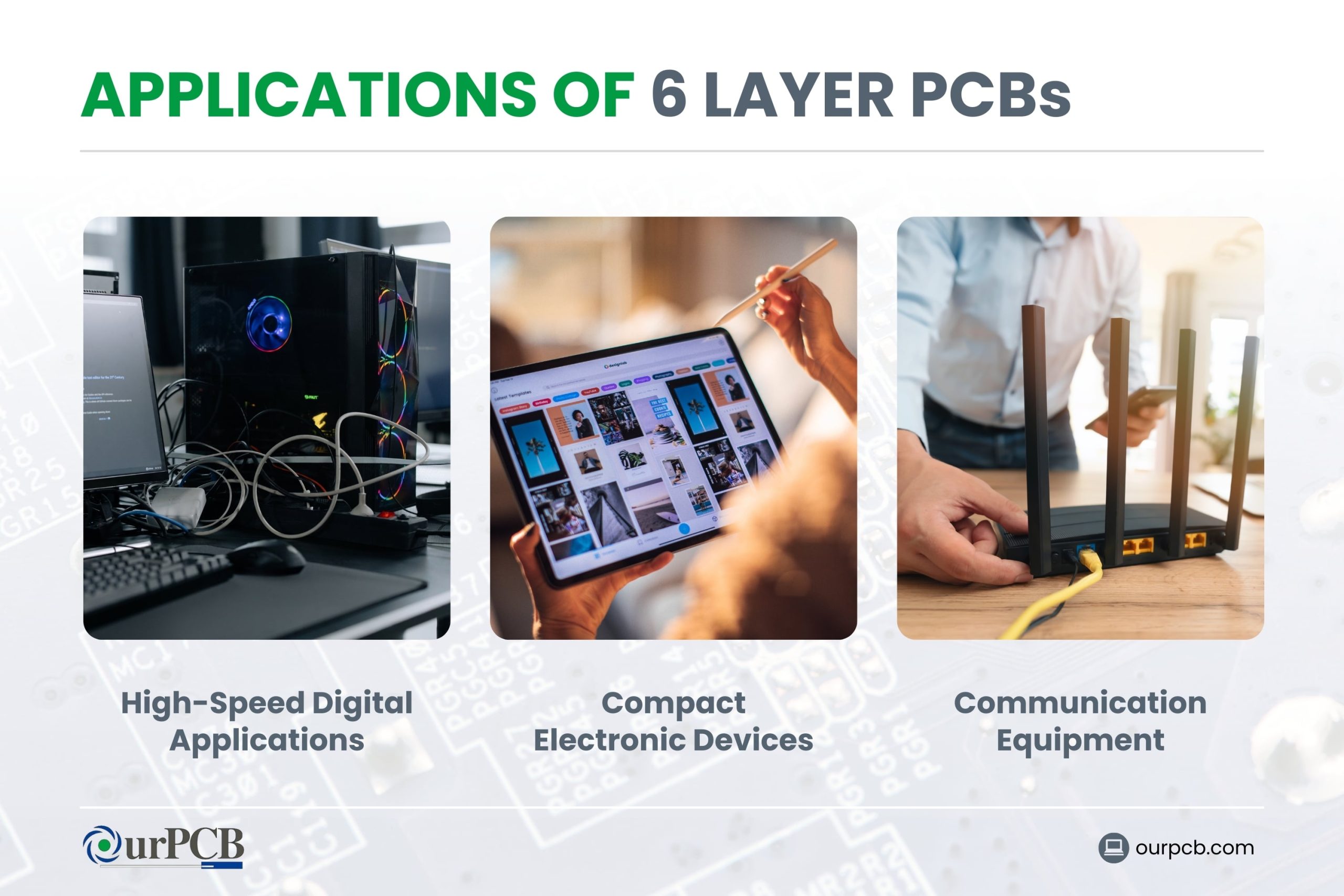

High-Speed Digital Applications
- Computer motherboards: 6-layer PCBs are used in motherboards that need complex routing to manage high-speed data transfer between the RAM, CPU, and other components.
- Graphics card: High-performance graphics cards use a 6-layer PCB to manage the connections between memory, GPU, and other components.
- Servers: They handle lots of data processing and storage, so a 6-later PCB helps maintain heat and improve power distribution.
Compact Electronic Devices
- Smartphones and tablets: Smartphones that have a lot of functions in a small-factor form also use 6-layer PCBs because they can handle many components and functions.
- Wearable devices: 6-layer PCBs support high functionality in a small and lightweight form, with proper connection and efficient power use.
Communication Equipment
- Routers: The additional layers in a 6-layer PCB handle multiple connections and high-speed data.
- RF modules: The multilayer structure supports the intricate routing needed for RF signals without losing the signal.
- Networking switches: The 6-layer PCB manages complex data routing.
Challenges in Designing 6-Layer PCBs
Thermal Management
Lots of heat can damage sensitive components of the PCB, which leads to loss of signal. Thermal expansion can crack the solder joints and delaminate layers.
The challenges are the compact designs make it hard to manage heat, so it needs thermal vias, heat sinks, and copper planes. Plus, selecting materials that conduct heat can be pricey.
Signal Integrity
High frequencies and speeds can cause crosstalk, attenuation, and reflection, leading to a loss of signal integrity. Designers must ensure that they put precise routing in place, which is complicated. Adequate grounding prevents noise and interference, and minimizing EMI requires strategic component placement and routing.
Cost vs. Complexity
Having many layers enhances functionality, but it increases costs. Complex routing needs very expensive tools and takes a long to develop, and high-performance materials cost more. However, the overall savings a 6-layer PCB brings is greater than other PCBs.
Comparison with Other Layer Counts
8-Layer vs. 6-Layer vs. 4-Layer PCBs
| 8-Layer | 6-Layer | 4-Layer | |
| Complexity | Highly complex, advanced applications | Moderately complex, balanced functionality | Less complex, simpler designs |
| Performance | Superior performance, more layers for routing and power | Good performance for most high-speed applications | Limited performance for lower-speed applications |
| Cost | Most expensive, complex manufacturing | Moderate cost, balanced with functionality | Most cost-effective, simpler, and higher yield |
6-Layer PCB FAQs
How is Power Routed on a 6-Layer PCB?
There is a dedicated power plane that ensures stable and efficient power delivery and, in turn, reduces voltage drops. Decoupling capacitors filter noise and provide continuous current, and proper power routing reduces EMI and noise. EDA tools optimize power distribution and allow precise placement and simulation.
When would you Need a 6-Layer PCB instead of a 4-Layer PCB?
If you have an application that needs high-speed or high-frequency signals, high component density, and advanced power management, then a 6-layer PCB is best.
Can a 6-layer PCB be Repaired When Damaged?
While a 6-layer PCB can be repaired, the process is very complicated due to the arrangement of layers. It would need specialized equipment, so skilled technicians would have to perform the repairs. Typical repairs include fixing broken traces, reworking solder joints, or replacing damaged components.
Back to top: What is a 6-layer PCB Stackup?
Special Offer: Get $100 off your order!
Email [email protected] to get started!