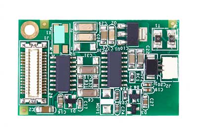
The performance of any modern electronic device depends on the internal components. One of these components is the 4-layer printed circuit board (PCB) stackup, a complex array for enhancing modern electronics’ capabilities. Whether you’re an engineer or a hobbyist, understanding the workings of a 4-layer PCB stackup can improve your project designs. Additionally, leveraging a PCB prototyping service can provide valuable insights and ensure your designs are optimized before full-scale production.
Contents
- What is a 4-Layer PCB Stackup?
- Key Advantages of Using a 4-Layer PCB Stackup
- Improves Signal Integrity
- Reduces Electromagnetic Interference (EMI)
- Better Power Distribution
- Ability for More Complex Routing
- High Component Density
- What Are Common 4-Layer PCB Stackup Configurations?
- Signal-Ground-Power-Signal
- Signal-Power-Ground-Signal
- Ground-Signal-Signal-Ground
- Signal-Ground-Ground-Power
- How Do Stackup Choices Affect PCB Thickness?
- What Are Some Successful 4-Layer Stackup Examples?
- Simple Designs
- Moderately Complex
- How Does a 4-Layer Stuckup Design Contribute to EMI Reduction?
- Dedicated Ground and Power Planes
- Controlled Impedance
- Strategic Layer Arrangement
- Use of Prepreg and Core Material
- What are the Important Design Considerations for a 4-Layer PCB Stackup?
- Layer Arrangement and Ordering
- Impedance Control
- Signal Integrity
- Crosstalk
- Power Integrity
- EMI/EMC Control
- Manufacturing Constraints
- Material Selection
- How are 4-Layer PCBs Manufactured?
- Inner Layer Printing and Etching
- Lamination of the Core and Prepreg Layers
- Drilling of Vias and Through Holes
- Copper Plating of Vias and Pads
- Outer Layer Printing and Etching
- Solder Mask Application
- Surface Finish Application
- Electrical Testing and Inspection
- What Factors Affect the Cost of 4-Layer PCBs?
- Board Size and Complexity
- Layer Count and Thickness
- Material Selection
- Quality and Production Volume
- Turnaround Time
- 4-Layer PCB Stackup FAQs
- How can you Optimize Signal Integrity in 4-Layer PCBs?
- How can you Optimize Power Distribution in 4-Layer PCB Stackups?
- Why Use a 4-Layer PCB Instead of a 2-Layer PCB?
What is a 4-Layer PCB Stackup?
A 4-layer PCB stackup is an arrangement of copper layers and insulating materials in a printedcircuit board (PCB) with 4 conductive layers. This arrangement ensures efficient power distribution and minimizes crosstalk, noise, and electromagnetic interference for a reliable signal. Typically, most standard 4-layer stackups come in the order below:
- First, a top signal layer on which you mount and connect components for signal routing.
- Next is the grounding plane, which offers the signal’s return path, reducing noise and interference.
- Third is the power plane, which distributes power to different board sections for a stable current supply.
- Lastly, there’s another signal layer at the bottom. You may also use it for mounting components.
Generally, a 4-layer PCB stackup offers better electrical performance than a 2-layer one, thanks to its dedicated power and grounding planes. It’s also inexpensive and less complex to manufacture than 6-layer and 8-layer stackups.
Key Advantages of Using a 4-Layer PCB Stackup
Improves Signal Integrity
Unlike a 2-layer board, a 4-layer arrangement isolates the grounding and powering plane and then sandwiches them between the bottom and top layers. Doing so allows for a continuous low-impedance path for signals, reducing crosstalks and reflections.
Reduces Electromagnetic Interference (EMI)
can cause noise and disruption of signals in any electronic device. The dedicated grounding acts as a shield to absorb and redirect electromagnetic waves away from the signals. Since the power and grounding planes are close, there’s also a decoupling effect, which reduces EMI even more.
Better Power Distribution
The isolated power plane in this kind of board also helps supply a stable and uniform voltage to different sections. As a result, there’s reduced voltage drop and noise, leading to enhanced power distribution across the board.
Ability for More Complex Routing
Separating ground and power from the bottom and top layers means there’s no routing conflict while simplifying the layout. You have dedicated routing layers, which are useful for complex high-speed circuits requiring precision.
High Component Density
With two isolated layers of signals, a 4-layer PCB stackup can handle higher component density compared to the 2-layer PCB. You can use the extra layers for routing, clearing space in the outer layers for more components. This allows you to create compact but efficient designs.
What Are Common 4-Layer PCB Stackup Configurations?
Here are some common 4-layer PCB stackup designs you can use depending on your application requirements:
Signal-Ground-Power-Signal
Here, the ground and power are sandwiched between signal routing layers. This is the most common configuration, since it strikes a good balance in many applications and offers a low-impedance return path, reducing signal noise and crosstalk.
You’ll also get efficient and stable power distribution across your board. While this design has a variety of applications, it’s most useful where you need high signal integrity and power distribution. However, although it balances power and signal, it may not work optimally with high-speed signals.
Signal-Power-Ground-Signal
In this design, the power is near the upper signal while the ground is close to the bottom signal. With power closer to the top signal layer, you can improve signal delivery and enhance power integrity. It also provides enhanced power supply to high-demanding components while preventing signal interference.
Expect to find this configuration in devices with high power requirements, since having the power close to the signal layer reduces voltage drop. While it improves power delivery, it may bring more noise to the top signal layer compared to the first configuration.
Ground-Signal-Signal-Ground
This design features two signal routing layers sandwiched between two ground layers to provide continuous grounding. In this case, the result is low impedance paths for returning current minimizing signal interference. When you sandwich a signal layer, you also get stripline routing ensuring minimized crosstalk and high signal integrity.
These stackup configurations are seen in high-speed circuits requiring minimal crosstalk and interference, like radio frequency and communication gadgets. Although they reduce EMI and provide excellent signal integrity, their manufacturing is expensive and complex.
Signal-Ground-Ground-Power
In this design, you have two ground layers for enhanced shielding and noise reduction. You also have a dedicated power plane for devices that demand extensive power. The result is a board with a stable power supply, as well as enhanced signal integrity.
You can find such boards in analog circuits and mixed signal devices where noise reduction and power are vital. However, they’re rare and may be costly to produce.
How Do Stackup Choices Affect PCB Thickness?
The stackup choice you make affects the thickness of your PCB, which in turn affects its mechanical functionality and fitment. The type of core and prepreg material you choose, plus the copper layers, significantly contributes to PCB’s thickness.
Layers affect the mechanical properties of your PCB, as well as its durability. PCBs with many layers are more durable yet less flexible, while flexible PCBs are thin ones but more susceptible to damage.
It’s vital to find a balance between flexibility and functionality when it comes to layer choices. Also, note that the thickness affects your connectors’ height and the devices you can connect to your PCB.
Special Offer: Get $100 off your order!
Email [email protected] to get started!
What Are Some Successful 4-Layer Stackup Examples?
Simple Designs
Imagine a device with a microcontroller, a sensor, an LED, and a power supply. This design requires a stable power supply, minimal interference, and efficient signal routing. Since you don’t need high-speed data transmission, you can go for a 4-layer stackup PCB featuring a signal-ground-power-signal design.
The advantage of choosing such a design is that it’s straightforward and inexpensive to manufacture. Its layer arrangement also ensures reduced interference for signal integrity and a dedicated reliable power supply.
Moderately Complex
Consider a small field programable gate array (FPGA device), or a similar device with many high-speed interfaces such as HDMI, USB, or ethernet. This kind of design requires signal integrity, minimal EMI interference, complex routing, and reliable power for high-speed transmission support.
You can go for a design like signal-ground-ground-power. The dual ground layer provides excellent EMI shielding for high signal integrity. Having the ground close to the signal layer offers crosstalk reduction and minimized signal reflection. You also have dedicated power at the bottom for noise-less power distribution for high-speed signal support.
How Does a 4-Layer Stuckup Design Contribute to EMI Reduction?
Dedicated Ground and Power Planes
A 4-layer board features a dedicated power plane and ground. Here’s how they help reduce EMI:
- Shielding: The ground plane shields your board from EMI that may interfere with your signals. This kind of PCB board also features an isolated signal layer that reduces external noise and EMI susceptibility.
- Reference Plane: Both the power and ground planes offer a stable reference point that minimizes interference. The ground plane provides a continuous low impedance for return current, ensuring stability and reliability in transmission.
- Capacitive Coupling: Having power and ground plane close also produces a capacative coupling effect. As a result of this, your board gets a decoupling mechanism that filters noise from the power line while boosting EMI immunity.
Controlled Impedance
Controlled impedance is also vital for preventing transmission errors and signal reflections that bring about EMI.
- Impedance Matching: When your board matches signal impedance with that of the transmission line, you reduce reflections and maintain signal integrity.
- Optimization Technique: You can alter the thickness and dielectric properties of the board layers to get impedance matching your application. Doing so reduces EMI and enhances your board’s effectiveness.
Strategic Layer Arrangement
You can arrange your layers strategically to suit certain applications, which can help reduce factors such as EMI.
- Minimizing Crosstalk: Place signal layers close to the ground plane to ensure the ground is the low-impedance path for return current. Making sure there’s enough separation between high-speed signals ensures reduced crosstalk and interference.
- Symmetrical Layout: A symmetrical arrangement maintains the structural and electrical balance necessary for EMI reduction.
Use of Prepreg and Core Material
The material you choose for the core and prepreg also can reduce the EMI effect based on their dielectric properties. Choosing materials with low-loss tangents and dielectric constants reduces signal attenuation while enhancing insulation.
What are the Important Design Considerations for a 4-Layer PCB Stackup?
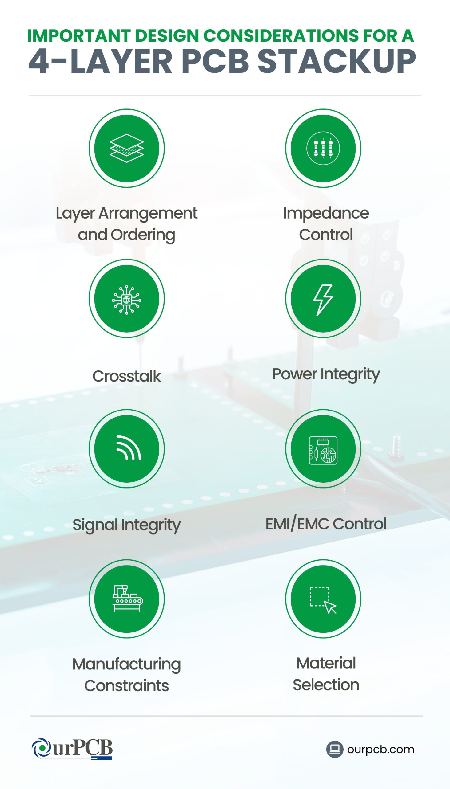
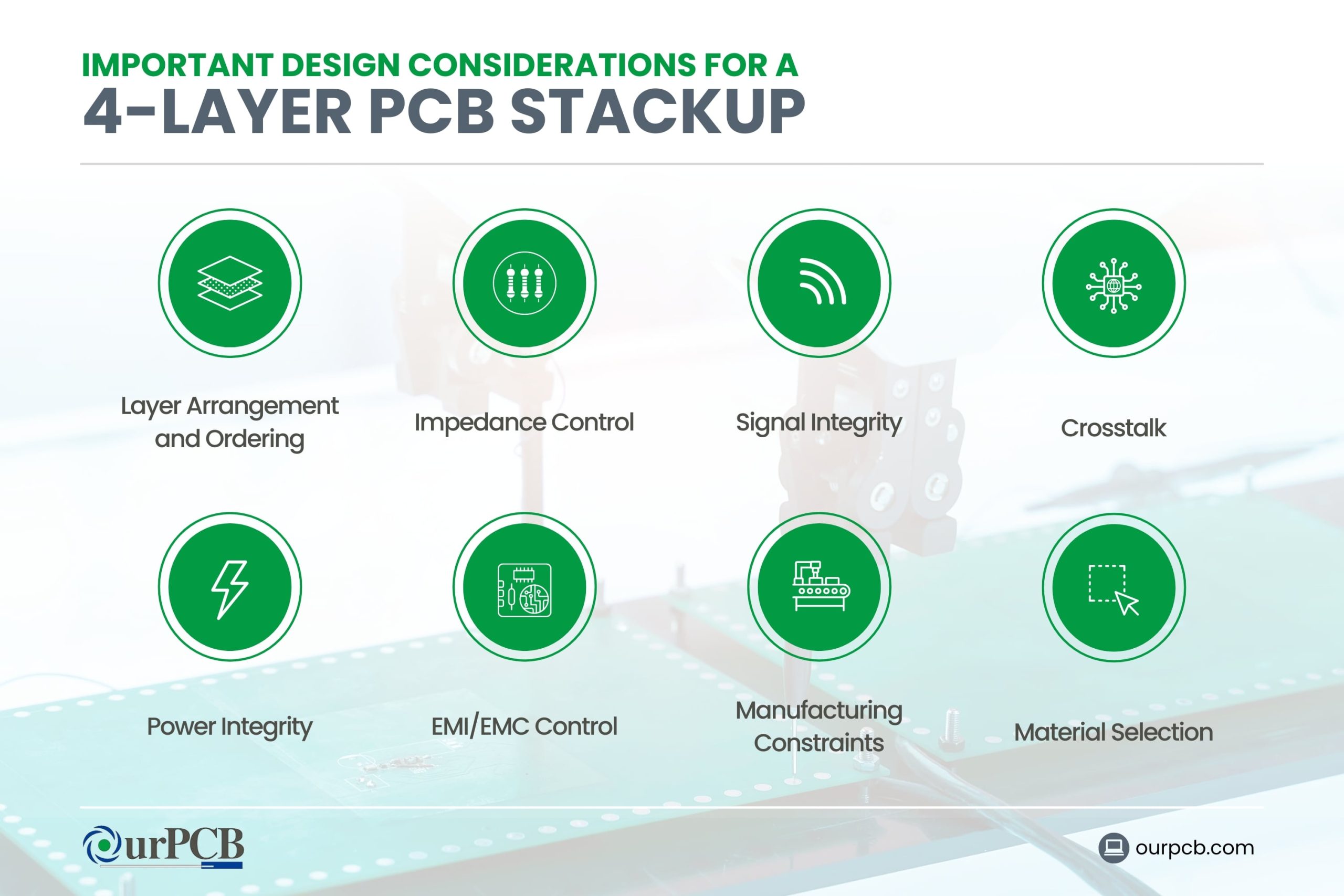
Layer Arrangement and Ordering
Consider EMI reduction, power distribution, and signal integrity when going for a certain arrangement. For instance, a signal-ground-power-signal arrangement may be suitable where you need good power distribution and signal integrity.
Impedance Control
When you control impedance accurately, you minimize reflections and errors that cause signal degradation, giving you reliable transmission. You can easily do this by adjusting the thickness of the dielectric layers and the signal trace width.
Signal Integrity
The first strategy for achieving signal integrity is reducing the signal path length. A short path reduces signal loss noticeably more than long ones, especially in high-speed devices.
Secondly, you can use differential signaling, where signal pairs reduce noise, carry data, and minimize external interference. Lastly, you could arrange your layers with signal layers close to the ground layers for a low-impedance path for return signals, reduced noise, and crosstalk.
Crosstalk
To minimize crosstalk, place signal layers near the ground plane to reduce interference. Another way is to use routing methods like perpendicular routing in all adjacent layers, keeping proper spacing between traces.
Power Integrity
To achieve a stable power distribution, isolatie the power plane for reduced noise and stable voltage reference. You can also use a decoupling capacitor near your power pins to filter noise and stabilize power. Lastly, ensure enough width for power traces, since wide traces can handle voltage efficiently without a drop.
EMI/EMC Control
Using a proper grounding technique can result in a solid grounding that minimizes interference and noise. Make sure the design and layer arrangement minimizes EMI emissions and susceptibility.
Manufacturing Constraints
Knowing and following manufacturing constraints can help you create designs that are simple and cost-effective to make. For instance, it’s vital to observe precise vias drilling for layer connections. Also, proper trace width and spacing ensure your boards meet their application requirements.
Material Selection
The material you choose determines the performance and manufacturability of your PCB prototype. When choosing the materials, consider heat stability, moisture resistance/absorption, and dielectric properties. Choosing an appropriate material boosts signal integrity, reduces losses, and improves functionality in various applications.
In addition to the above considerations, you can also read our PCB Design tips article to get more information on designing PCBs. Otherwise, consider our PCB Design services to make it easier for you.
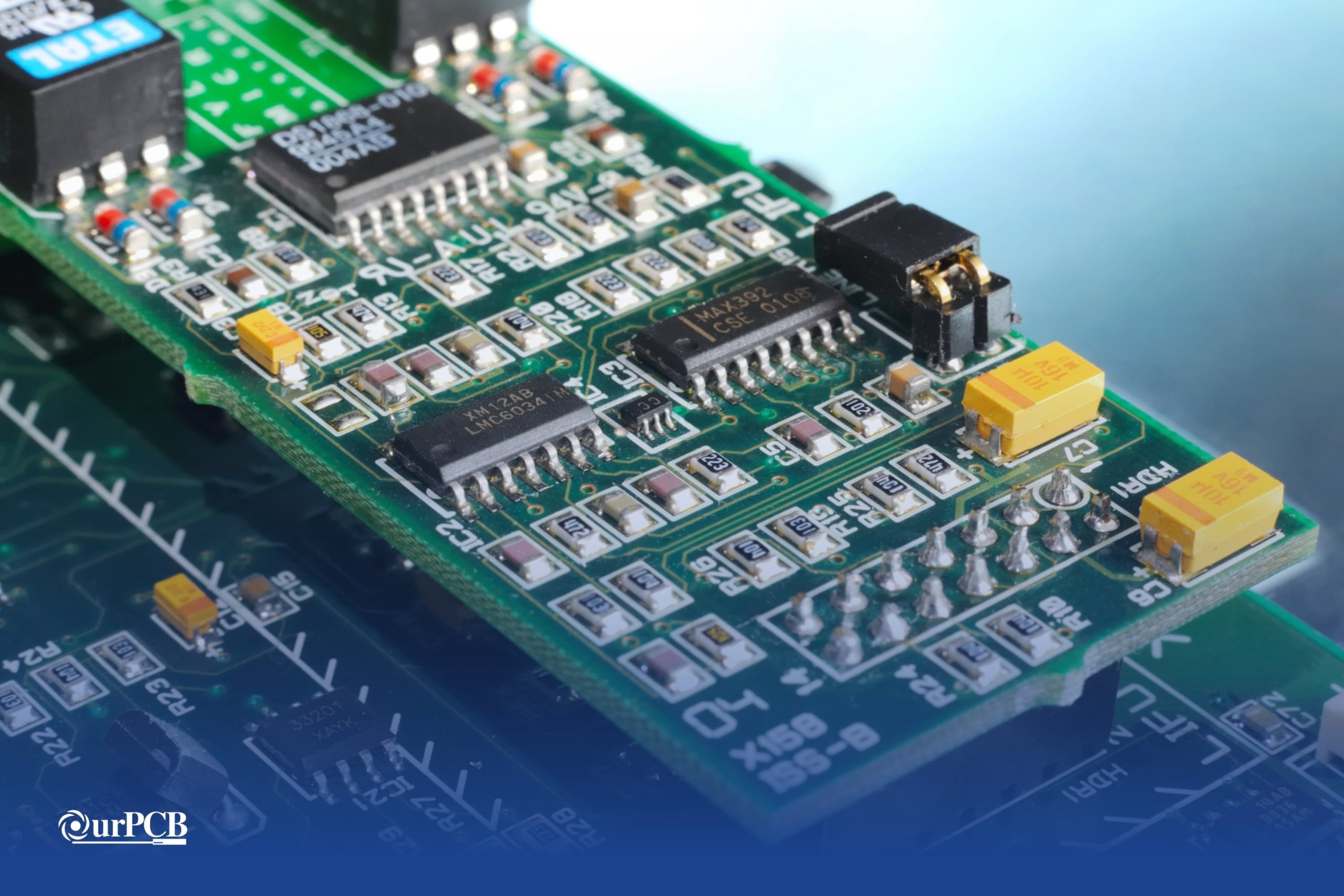
How are 4-Layer PCBs Manufactured?
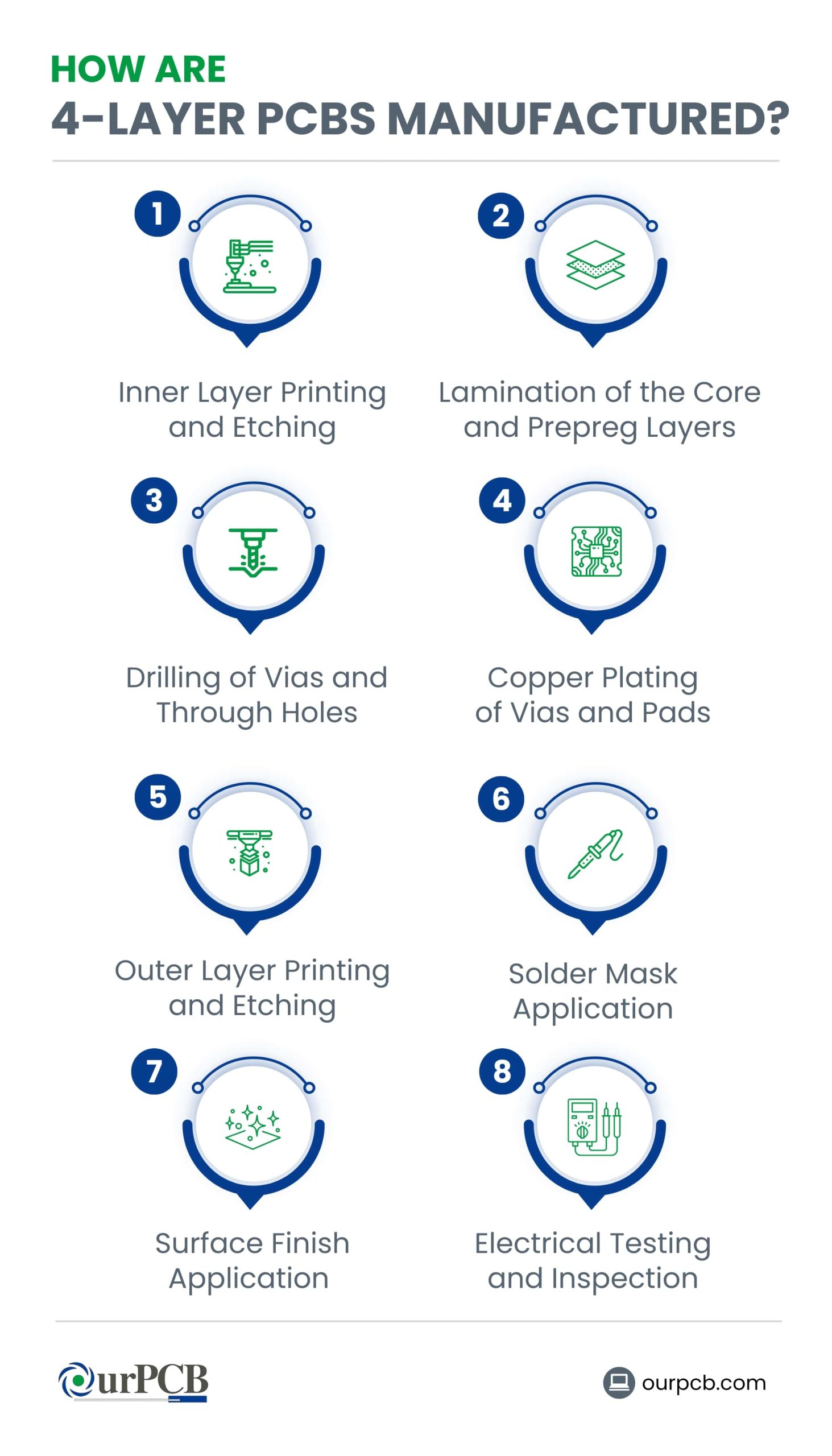
Inner Layer Printing and Etching
The manufacturing process starts by placing photoresist layers on the inner copper layers to offer protection for subsequent steps. From there, manufacturers use UV light exposed film to transfer the circuit partner they want to the photoresist.
The exposed photoresist areas are developed, leaving the planned copper traces behind. They then etch the excess copper and leave the circuit print on the inner layer of the board.
Lamination of the Core and Prepreg Layers
Once the inner layer is printed and etched, the manufacurer aligns the core and prepreg to the inner copper layer. The process ensures proper layer positioning before lamination. In the laminate machine, the board endures high temperatures and pressure. Here, the prepreg resin melts and binds the layers, forming a durable and reliable board.
Drilling of Vias and Through Holes
In this step, the vias and through holes are drilled using CNC machining to ensure precision. These holes are strategically placed depending on the board design to ensure different layer and components connection. From there, the hole edges get deburred to remove any sharpness that can damage traces.
Copper Plating of Vias and Pads
After drilling, holes are copper-plated for enhanced conductivity. The plating process involves first cleaning the hole with chemicals to get rid of contaminants, then installing a thin copper layer on the hole walls using the electroless copper deposition technique. From there, the electroplating process adds to the copper layer thickness for desired conductivity.
Outer Layer Printing and Etching
This step involves printing the desired circuit pattern on the outer layer and etching it. This ensures the circuit pattern is present in both the inner and the outer layers.
Solder Mask Application
Once they have the desired circuit pattern, manufacturers apply a solder mask to the traces on the board. This ensures protection of the copper traces while only exposing the desired areas for component soldering. Then, the board is cured using UV or heat to harden the solder mask and prevent oxidation of traces.
Surface Finish Application
In this step, manufacturers apply various methods to protect the exposed traces from elements and improve soldability. These may include hot air solder leveling, electroless nickel immersion gold, and organic solderability preservatives. The finishes above are applied using electroplating, emersion, or chemical techniques, depending on the desired design finish.
Electrical Testing and Inspection
At the end of the manufacturing process, each device goes through automated tests to ensure circuit continuity. This process includes a meticulous visual inspection to detect any deformities and assess overall quality. From there, only PCBs that pass the testing get prepared for shipment.
What Factors Affect the Cost of 4-Layer PCBs?
Board Size and Complexity
Bigger boards require more materials and more time to complete, increasing production costs. Complex designs also require specialized machining and handling, which come at a higher price.
Layer Count and Thickness
Thicker PCBs with many layers increase cost due to more material usage, as well as labor costs for the increased time spent manufacturing.
Material Selection
Special materials such as high-speed laminate for specialized boards come at a premium price. Certain materials may also be harder to source, increasing their price tag.
Quality and Production Volume
Typically, large production costs less per unit since you can buy materials in bulk and use equipment and labor efficiently. On the other hand, the initial cost can be expensive for small orders.
Turnaround Time
Fast turnaround time calls for extra shifts and production priority, which comes at an increased cost. Rush orders may increase production costs, which manufacturers add to the customer’s final bill.
4-Layer PCB Stackup FAQs
How can you Optimize Signal Integrity in 4-Layer PCBs?
The first thing to improve signal integrity is to match signal requirements with trace impedance to reduce reflection. You can also shorten trace lengths to prevent signal loss. Lastly, you can use a strategically placed ground to offer a return path for signals, reducing noise.
How can you Optimize Power Distribution in 4-Layer PCB Stackups?
For power distribution optimization, you can use decoupling capacitors to filter high-frequency noise and stabilize the voltage. You can also maintain stack symmetry and use thinner dielectrics for controlled impedance.
Why Use a 4-Layer PCB Instead of a 2-Layer PCB?
One of the main pros of using a 4-layer PCB over a 2-layer is the isolation of ground and power ensuring signal quality. It also comes in handy for complex routing thanks to the space in the extra layers.
Designing your own 4-layer PCB stackups? Contact us today and get a free quote in seconds.
Back to top: What is a 4-Layer PCB Stackup?
Special Offer: Get $100 off your order!
Email [email protected] to get started!