


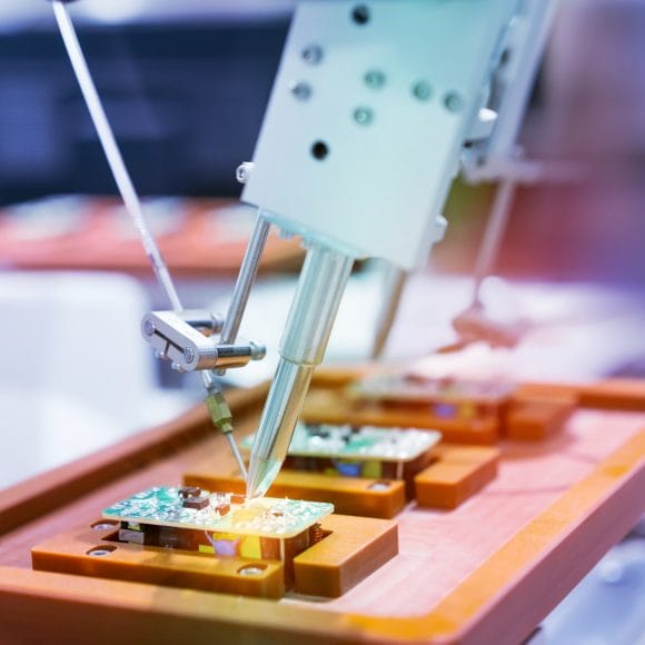
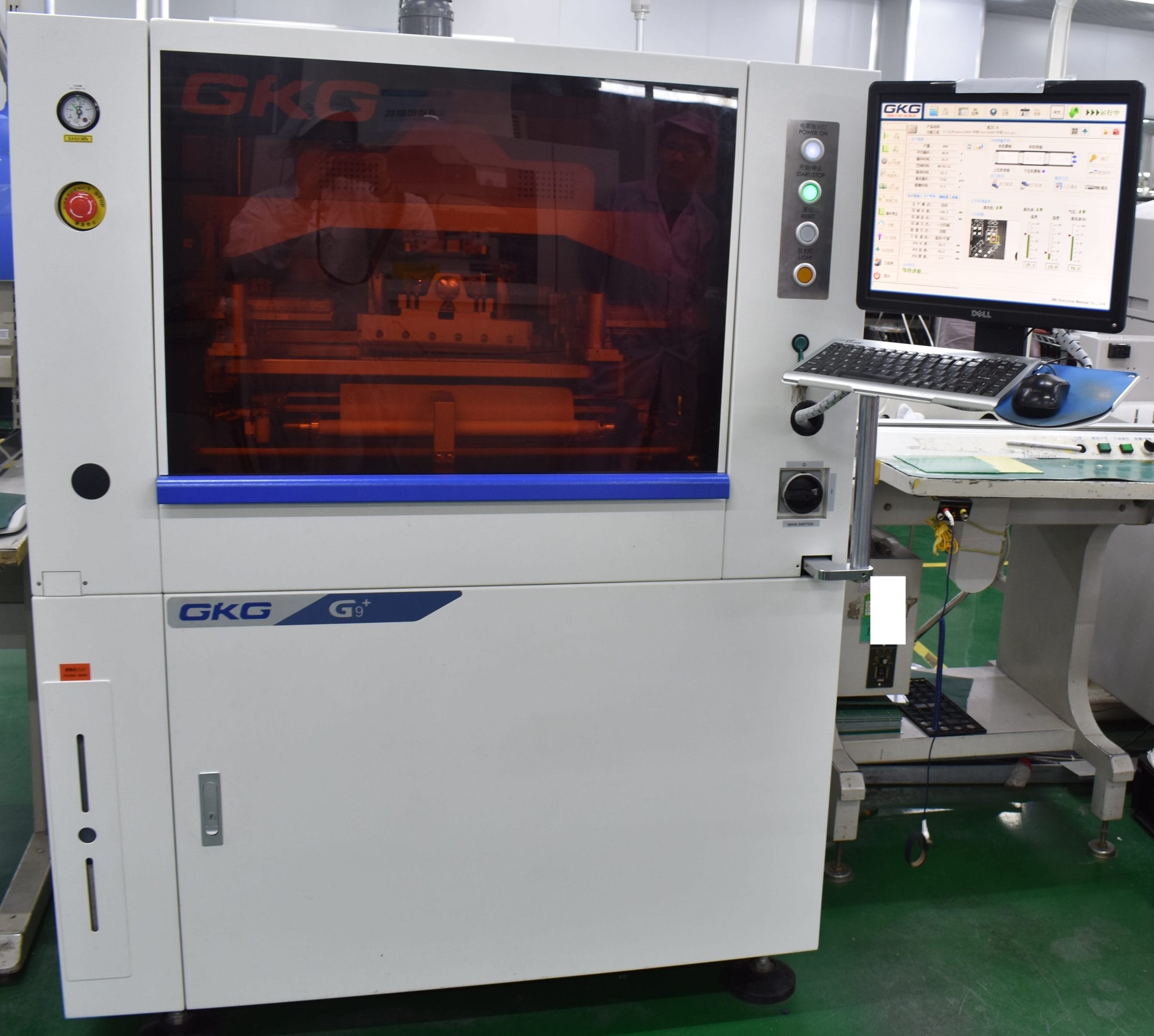
We handle everything from parts sourcing to final assembly, providing a hassle-free experience that ensures top-quality boards every time.
Whether you need a few prototypes or large-volume batches, our flexible assembly services adapt to your project’s scope and timeline.
Stay environmentally responsible with our compliant assembly processes, offering RoHS and lead-free options for safe, reliable builds.
No matter the complexity, we can assemble boards of all configurations—single-layer, multi-layer, or a mix—to match your exact specifications.
From one-off prototypes to bulk orders, we accommodate projects of all sizes without compromising on quality or turnaround time.
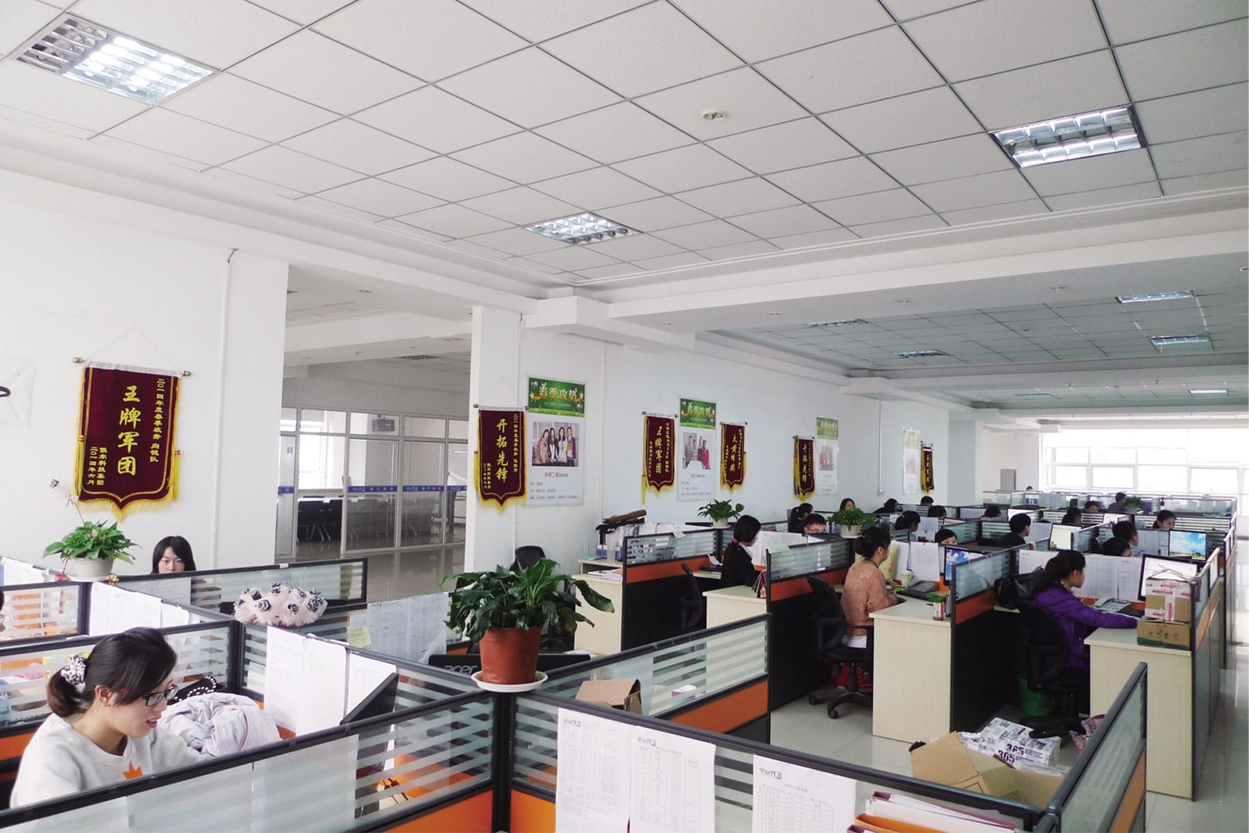
Join our growing community of satisfied clients who rely on our dependable assembly expertise and dedicated customer support.
Mon-Fri: 24 hours,
Sat: 9am-6pm, GMT+8
Reach us at
sales@ourpcb.net
24 hours online
+86-199-30589219
Mon-Fri: 24 hours,
Sat: 9am-6pm, GMT+8
Order options
Quick-turn RF prototypes with material characterisation and DFM review.
Low-volume high-frequency production with impedance testing.
Scaled high-frequency manufacturing with full parametric testing.
★ What customers say
They hit an aggressive deadline on our high-frequency boards and still nailed the quality.
The review team caught a stackup problem on our high-frequency boards early.
The high-frequency boards came back flawless — tight tolerances and a clean soldermask finish.
Competitive quote on the high-frequency boards with no surprise costs.
Clear, fast updates the whole way through the high-frequency boards order.

