A trace is a general term for all copper or transmission lines used in PCBs. However, high-frequency circuit boards require unique transmission lines that minimize losses.Striplines and microstrips are the most typical high-frequency transmission lines, and we will do a stripline vs. microstrip comparison to determine the best applications for each one. Take a look!
Contents
- What is a Stripline?
- Stripline Routing Styles
- Characteristic Impedance of a Microstrip Line
- Stripline Design Considerations
- Advantages of Strip lines
- Limitations of Strip lines
- Losses in Strip lines
- What is a Microstrip?
- Microstrip Routing Styles
- Characteristic Impedance of a Stripline
- Propagation Mode in Microstrips
- Advantages of Microstrips
- Losses in Microstrips
- Stripline vs. Microstrip: The Differences
- Stripline vs. Microstrip: Which Transmission Line is Better for Routing?
- Microstrip vs. Stripline vs. Coplanar Waveguide
- Stripline vs. Microstrip: Which One Should You Use?
- Wrap Up
What is a Stripline?
A stripline sits inside the substrate material with two ground planes sandwiching it and the substrate.
This impregnation implies the transmission line can only exist in internal PCB routing layers (three board layers minimum).
Therefore, striplines are prevalent in multi-layer circuit boards, and the arrangement shields the stripline while minimizing emissions.
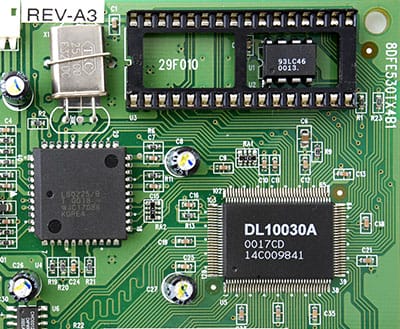
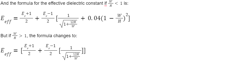
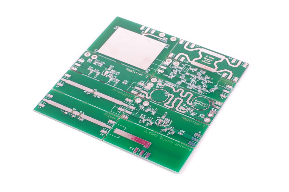
A radio frequency and microwave PCB
Stripline Routing Styles
Striplines have the following routing techniques.
Symmetric Stripline
Also known as a plain stripline, the symmetric stripline features a signal trace routed between two reference planes. Its impedance calculation model uses the trace's width & thickness and dielectric substrate type & thickness as parameters.
Asymmetric Stripline
This stripline resembles the symmetric stripline structurally, but the trace is not in the middle/centrally placed between the ground planes.
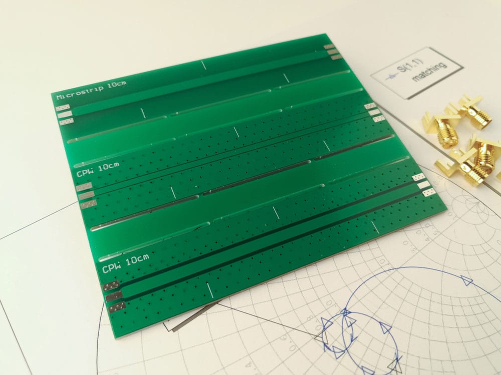
A high-power radio frequency PCB
Broadside-Coupled Stripline
This technique routes the striplines as pairs in the internal layer, with one line above the other in parallel.
Edge-Coupled Stripline
Instead of placing the traces in parallel vertically, edge-coupling places them side by side in parallel. They can be symmetric or asymmetric.
Characteristic Impedance of a Microstrip Line
A microstrip’s characteristic impedance changes as you increase or decrease the signal’s frequency, but is affected by these factors.
- Substrate material’s dielectric constant: This is the ratio of the capacitance of a capacitor with a dielectric that is the test material to the capacitance of a capacitor with air or vacuum as the dielectric.
- Effective dielectric constant: Some of the electric fields produced by the microstrip form in the air, which means the electric energy storage occurs in the substrate and the air. The effective dielectric constant is a function of the ratio of the microstrip’s width to height and the dielectric material’s relative permittivity.
- Capacitance: The capacitance between the microstrip and the ground plane also affects the characteristic impedance, where an increase in capacitance lowers the line’s impedance.
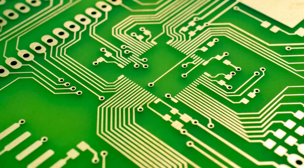
Copper tracks on a printed circuit board
- Dielectric substrate thickness (height): The dielectric’s height also affects its capacitance, where an increase in thickness increases the capacitance, which lowers the impedance.
- Trace width: The microstrip’s width includes the copper foil and its metal coating. Thick trace widths have a lower impedance than narrow ones.
- Trace thickness: A conductor’s thickness affects impedance the same way as width, whereby an increase in thickness reduces the resistance, which lowers the impedance, provided the reactance remains constant.
Microstrip Characteristic Impedance Formula
All these factors come together in the characteristic impedance formula, which is as follows.

Where:
- Z0 is the characteristic impedance in ohms
- Er is the substrate’s dielectric constant
- Ln is the transmission line’s length
- W is the copper trace width
- T is the transmission line’s thickness or height
- H is the distance of the microstrip from the ground plane
These variable measurements are in mils, and the equation is most accurate when the characteristic impedance is between 50 and 100 ohms.
But we’ve not covered the effective dielectric constant and capacitance.
Microstrip Characteristic Capacitance Formula
The formula for the characteristic capacitance is:

Microstrip Effective Dielectric Constant Formula
Stripline Design Considerations
Striplines have three conducting layers, with the sandwiched signal conductor embedded in an isotropic and homogeneous dielectric featuring a dielectric constant Er.
In a defined time and cross-section, the electric field lines for the fundamental TEM mode in striplines move outwards from the signal conductor to the ground planes.
On the other hand, magnetic field lines revolve around the inner conductor.
In TEM (Transverse Electromagnetic) mode, the signal/inner conductor is at the same potential (equipotential). The region between the outer conductor and the stripline has a single medium.
Therefore, the fundamental TEM's characteristic impedance and phase velocity do not vary with frequency.
Advantages of Strip lines
- Shields and protects the signal layer
- Low impedance (reduces crosstalk and emissions)
- Better EMI characteristics
- Noticeable improvement above 50MHz
Limitations of Strip lines
- Difficult to decouple
- Low impedance for proper matching
- Tough to debug embedded traces during prototyping and troubleshooting
Losses in Strip lines
- Magnetic resonance
- Finite conductivity of the conductors
- Limited dumping phenomenon and resistivity of the dielectric
What is a Microstrip?
A microstrip is a planar transmission line that sits outside the dielectric material. The PCB material insulates and separates the trace from its single ground plane, meaning the line has air above it.
Therefore, the transmission line can only exist on the upper and lower PCB layers. And the dielectric constant of air and the board material affect the trace impedance.
A microstrip RF transmission line in a microwave PCB
Microstrip Routing Styles
Microstrips have the following routing styles.
Microstrip
These signal traces sit on the exterior layers of PCBs, and their impedance calculation model depends on the trace width & thickness and dielectric type & thickness.
Edge-Coupled Microstrip
This transmission line resembles the edge-coupled stripline but with a single reference plane and external routing for the two traces.
Embedded Microstrip
An embedded microstrip is similar to a regular microstrip transmission line, but the trace has some dielectric material above it.
The additional dielectric material above the strip could be a solder mask.
Characteristic Impedance of a Stripline
The characteristic impedance of a stripline is rather straightforward because it varies depending on the geometry of the conductor and ground planes below and above it, and the substrate material’s dielectric constant. So here is the formula.

Where:
- b is the spacing between the planes
We is the conductor’s width.
Propagation Mode in Microstrips
The dominant signal propagation mode in microstrips is Quasi-TEM (Transverse Electromagnetic).
The phase velocity, field variation, and characteristic impedance (in the transmission line's cross-section) are frequency-dependent in TEM mode.
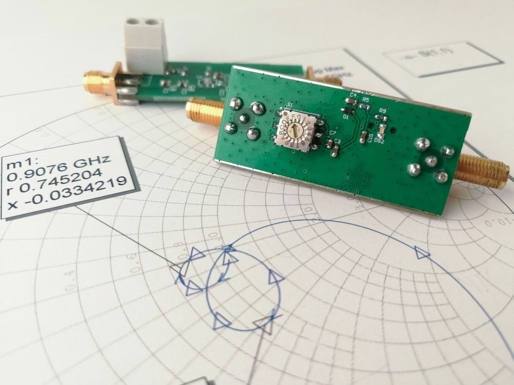
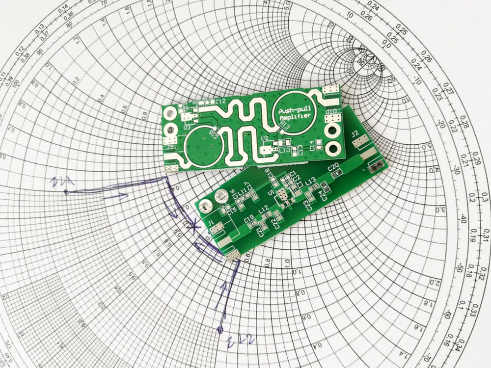
An RF PCB on a Smith chart for impedance matching
Advantages of Microstrips
- Easy to connect to components
- Creates minimal crosstalk when packed with multiple channels in a high-density design
- Minimally affected by PCB manufacturing process tolerances
- Faster propagation time
- Provides mechanical support and heat sinking simultaneously
Losses in Microstrips
- Radiation effects, depending on the dielectric substrate thickness, dielectric constant, frequency, and circuit geometry
- Dumping phenomenon and the substrate's finite resistivity
- Magnetic losses relevant to the magnetic substrate
- Line conductor's finite conductivity
How To Minimize Losses in Microstrips
The most effective way to reduce microstrip losses is to suspend the substrate in the air.
This suspension increases the separation between the signal layer and ground path, enhancing the trace's tendency to radiate at the discontinuities.
How does it work?
The air between the ground plane and the substrate bottom contains an electromagnetic field. Since air has zero dielectric losses compared to standard PCB substrates, it minimizes the insertion losses.
On top of that, the conductive trace's width increases due to the reduced effective dielectric constant. A narrow trace width increases losses, so the broader, the better.
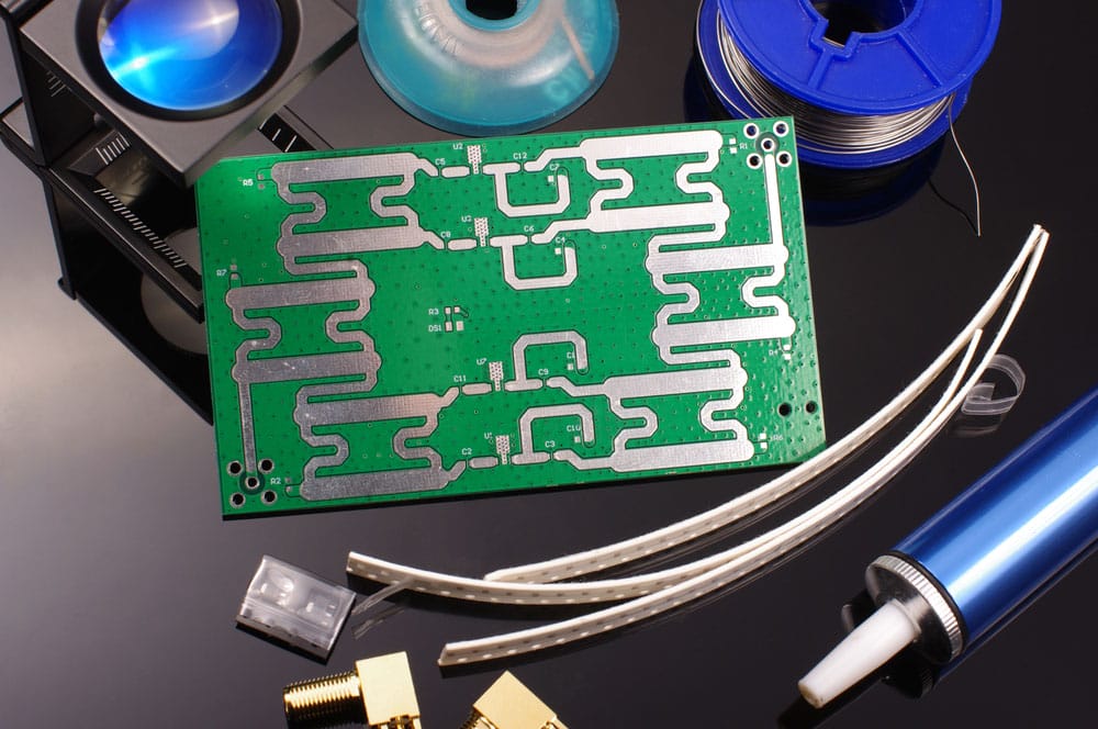
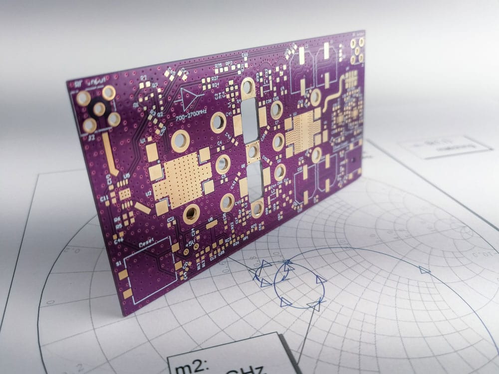
A high-frequency PCB
However, this air suspension technique is effective only up to a few GHz.
Special Offer: Get $100 off your order!
Email sales@ourpcb.net to get started!
Stripline vs. Microstrip: The Differences

Stripline vs. Microstrip: Which Transmission Line is Better for Routing?
One of the parameters required to calculate routing is the dielectric constant of the dielectric layer used in the PCB.
Microstrips
Routing microstrips above and below the board minimizes dielectric losses more than routing strip lines because air has negligible losses.
Additionally, it is simpler to fabricate microstrips because the conductor strip is on the outer layer.
However, microstrips radiate more energy due to exposure to air. The dielectric constant inside the PCB layers is usually 1.4, while that of air is 1. This variation explains the impedance value differences between strip lines and microstrips.
Exposed microstrips on an RF PCB
Strip lines
On the other hand, stripline routing has the advantage of sandwiching the signal traces between two reference planes.
This arrangement allows the fabrication of narrower signal lines for the same impedance values required for microstrip routing.
Also, the sandwiching creates better insulation by the dielectric material. So you can compress the routing.
Microstrip vs. Stripline vs. Coplanar Waveguide
Structurally, microstrips and coplanar waveguides are similar because they have the copper signal line on the dielectric.
However, coplanar waveguides have ground planes sitting on either side of the signal line on the same plane, hence the name coplanar.
Different PCB layer structures
However, some have an additional ground plane below the dielectric, while others have conductive via-holes linking the upper coplanar ground lines to the lower plane.
These two variations are known as coplanar waveguides with ground and grounded coplanar waveguides, respectively.
However, microstrips don’t have coplanar return lines. The signal line sits on its own above the dielectric, with the ground plane below the substrate.
On the other hand, striplines are signal conductors routed in the internal layers of circuit boards, where they are sandwiched and surrounded by the substrate. The return planes sit on either side of the dielectric.
Taking these structural differences into account, you won’t be mistaken to conclude that striplines are suitable for routing signals in the internal layers of multilayer circuit boards.
But you can place microstrips and coplanar waveguides on the inner or outer layers because they don’t sit in the middle of the substrate.
All three can handle high-frequency signal transmission in the radio frequency range, albeit with varying properties that suit specific applications.
Stripline vs. Microstrip: Which One Should You Use?
Each PCB transmission line has its benefits and drawbacks. Most modern high-frequency circuit boards with high-speed designs also require high circuit densities. So you will need a combination of both traces.
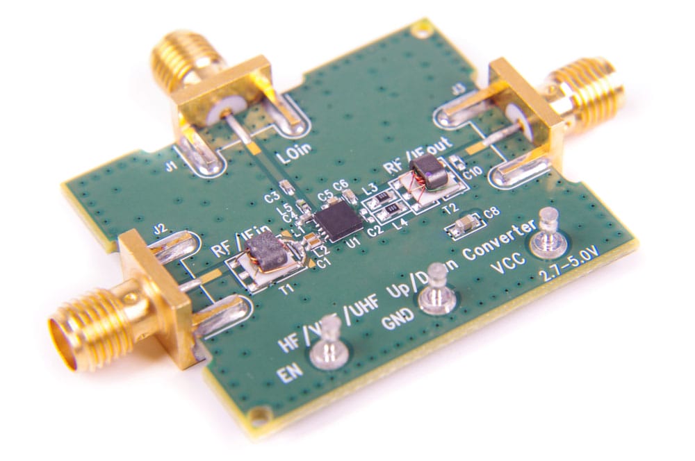
An RF microwave mixer evaluation PCB
Modern PCB tools can help simplify the microstrip and stripline routing configurations.
Impedance calculators can also help you determine the best trace width and layer configurations, while stack-up editors assist in plugging in the correct board widths and materials.
These tools combined can help you determine the best stripline or microstrip routing method and layer to configure with your routing layers.
Wrap Up
As you can see, striplines and microstrips have a simple structural difference that varies their properties greatly.
Each transmission line excels in certain areas, and you might have to incorporate both into your high-frequency PCB to minimize losses.
That's it for this article. If you have any questions or comments, leave a message, and we'll get back to you asap.
Special Offer: Get $100 off your order!
Email sales@ourpcb.net to get started!