Any circuit requires grounding to create a potential difference for current to flow. And it is particularly critical in PCBs because these circuits have several electronic components. But how do you ground PCBs properly? And how do you design this layer in your board layout? We will look at the ground plane PCB in detail to explain its functions and design guidelines below. Take a look!
Contents
- What Is a Ground Plane in a PCB?
- PCB Grounding Techniques
- Ground Plane
- Ground Vias
- Decoupling
- Connector Grounds
- Functions of a PCB Ground Plane
- Voltage Recovery
- Signal Recovery
- Reduce Noise and Interference
- Power Integrity
- Ground Plane PCB Design Guidelines and Their Connections
- Routing
- Multilayer Designs
- Connections
- Tips on How To Ground a PCB
- Wrap Up
What Is a Ground Plane in a PCB?
A ground plane in a PCB is a metal layer of copper foil in the board stack-up. The copper layer connects directly to the circuit ground, which is usually one terminal of the power supply. This ground layer acts as the return path for most components and current in the circuit.
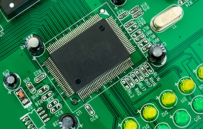
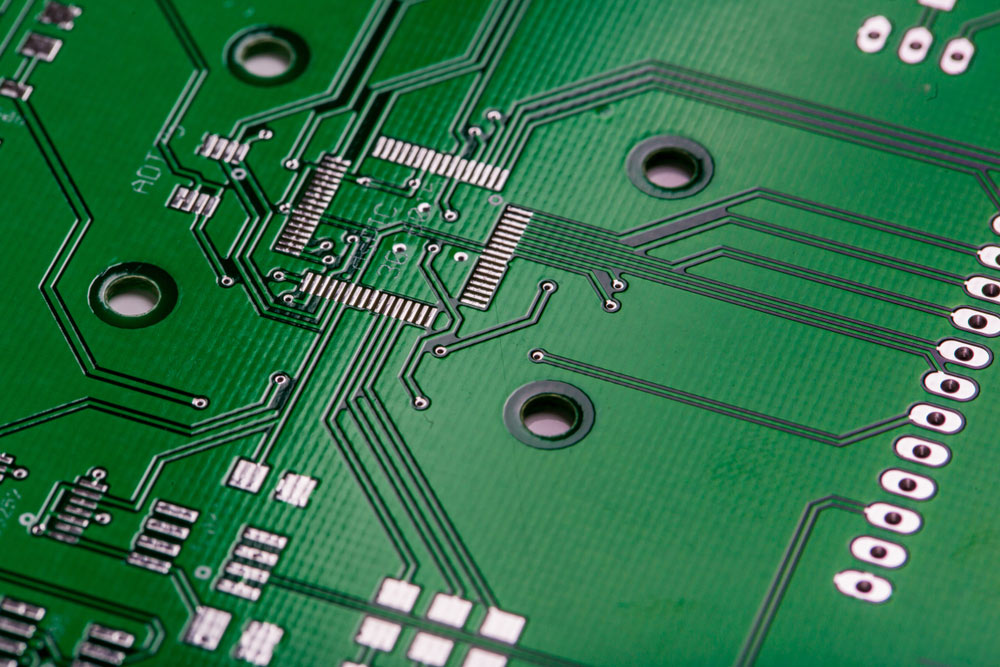
A radio frequency amplifier PCB with a plated-through via to access the ground plane
The ground plane layer can occupy a tiny portion of the PCB or an entire board layer. In some cases, it can take up multiple board layers. Exclusively occupying a single layer is advantageous because it simplifies the circuit layout. As a designer, you can ground any electronic component without routing ground traces. Instead, you route these component ground pins through a hole to get to the ground connection on a different layer.
PCB Grounding Techniques
You can use several techniques to ground a PCB, with the most typical ones including the following.
Ground Plane
As described above, this plane is a large piece of copper that covers all spaces without a trace or component. In a two-layer PCB, design rules indicate this plane should be on the bottom layer, with signal traces and electronic parts on the upper layer.
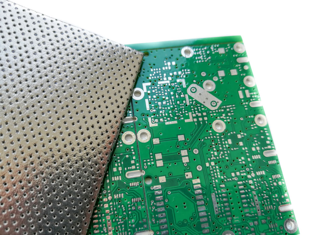
The bottom layer of a PCB with broad copper tracks
When using a ground plane, it is best to make signal traces as short as possible, then place the ground plane to cover the entire space under them. This design helps avoid the creation of a conductive ring that acts as an inductor and creates external magnetic fields that can cause a ground loop electric current.
This plane can also be on both sides of a board, with the one on the component side being at the supply voltage while the other one stays grounded. The design keeps the ground voltage at the same level across the board.
And you can use more than one ground copper plane on two-layer boards, but each one should connect to the power supply independently. This connection will prevent ground loops and keep the plane layers separate.
Ground Vias
These vias connect ground planes on different layers in multilayer PCBs to enable you to access the electrical ground from any part of the PCB. Also, they help prevent ground loops by providing a shorter path for the current to flow via a low-impedance path.
In some cases, copper pieces can resonate at one-fourth the frequency of the current flowing across. Placing stitching vias (via fence) at specific intervals around the ground plane will eliminate these oscillations by creating a capacitive path back to the ground.
An up-close image of a PCB with multiple vias
The general rule of thumb is to place them at an eighth of the wavelength or less from the conductor.
Creating these vias involves drilling through the PCB, passing thin copper wires, then soldering on each side.
Decoupling
Integrated circuit chips in PCBs require power to operate. These chips feature power pins that connect them to external power sources and ground pins to link them to ground planes.
A decoupling capacitor sits between the ground and power pins to smoothen oscillations in the voltage supplied to the chip. This capacitor stores charge to power the IC when it needs additional current via a low inductance path. So the best place to position this capacitor is close to the IC's power pins.

An electrolytic radial decoupling capacitor
The capacitor also helps reduce EMI and minimize the noise going into the ground & power plane pairs. This noise could be due to the following:
- The decoupling capacitor does not provide sufficient current, which lowers the IC power pin voltage
- Intentional current being sent between the ground and power planes with a fast-switching signal using a via hole
So it is best to distribute the capacitors across the board, with some near the IC power and ground pins. Also, use a capacitor's highest value and keep all of them at the same value.
Connector Grounds
All PCB connectors should have a link to the ground. And all signal conductors must run in parallel, so you must separate them using ground pins. PCBs usually need more than one conductor leading to the ground. And having a single connector pin may cause impedance mismatch issues that cause oscillations.
The back-and-forth bouncing of the current can affect system performance and may raise the connector pin's contact resistance over time.
So use several ground pins. And they should be about 30-40% of the total PCB connector pins.
Special Offer: Get $100 off your order!
Email [email protected] to get started!
Functions of a PCB Ground Plane
The ground return path has four primary functions.
Voltage Recovery
Circuit boards house multiple parts, and over 90% connect with a power net when running. So the voltage appears via the ground net. And the designer needs to use wider traces if the multilayer circuit board has less than four layers.
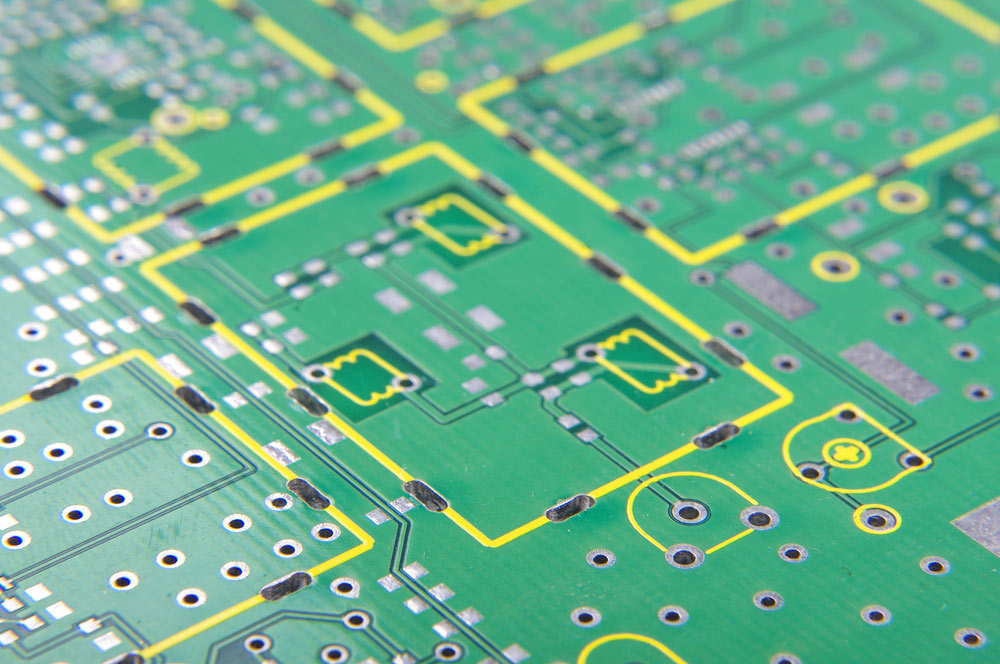
A PCB with multiple traces
A multilayer PCB stack-up with over four layers needs more attention, so the fabricator must use a high-quality sheet for the ground plane. The goal is to create a reliable connection between the ground nets and the circuit components.
Signal Recovery
A track might engage the other via electromagnetic induction if two signal traces run parallel. This engagement creates electromagnetic interference because there are no clear paths for the signals to return. But a ground trace ensures the electrical signals return without interfering with other circuit parts.
Reduce Noise and Interference
A large quantity of energy usually discharges via the ground circuit when a shift occurs in the digital circuit position. This action creates noise and interference that you can avoid by integrating the ground planes.
A PCB with a special-purpose shielding material
Power Integrity
The components in circuit boards draw a lot of power when in operation. The ground plane helps smoothen power spikes created by this operation.
Ground Plane PCB Design Guidelines and Their Connections
The following recommendations are critical when using circuit board design tools to create ground copper planes.
Routing
Route the ground layer using the widest trace for single-layer boards. And it is advisable to design the ground plane to provide electrical benefits.
Multilayer Designs
Multilayer circuit boards require stack-ups with the correct ground layer and layer width configuration for proper routing. Also, you can design effective PCB ground planes as positive or negative images with additional area fills for the ground.
Connections
SMT pad traces to via grounds should be wide enough to lower their inductance. But avoid using broad traces on tiny, discrete parts.
Tips on How To Ground a PCB
Every PCB design needs grounding, and you should follow these grounding practices.
- Ensure you attach everything and fill any open space with copper and vias that connect to the ground plane
- Keep the ground layer whole to avoid ground current loops
- Have a single-point grounding, such as the board's chassis, metal frame, or dedicated ground layer
- Reduce the usage of series vias along ground paths because they create impedance
- Do the grounding design before routing because it is the foundation of the routing process
A close-up of the PCB design layout routing process using CAD software. Note the ground thru holes
- Understand how currents flow in the board to ensure proper grounding
- Keep analog and digital signal considerations in mind when planning the grounding
- Plan for dynamic variance when sending ground connections between boards in multilayer PCBs
Wrap Up
In conclusion, ground plane PCBs are critical layers in PCB layouts, but you must design them correctly to make them fully functional and beneficial to your circuit board. The design guidelines and tips described above should help you in this process. But if you encounter any challenges, contact us, and we'll sort you out.
Special Offer: Get $100 off your order!
Email [email protected] to get started!