Contents
- What Is a PCB Stackup?
- Why is the PCB Stack-up Important?
- PCB Stackup Requirements
- Foil Construction vs. Cap Construction
- Board Component Density (Number of Layers and Spacing)
- What Materials are Used in PCB Stackups?
- Copper for Conductive Layers
- Prepreg and Core for Insulation
- Special Materials for High Frequency Applications
- What are the Challenges in PCB Stackup Design?
- Managing Cross-Talk Between Closely Packed Traces
- Ensuring Impedance Control Across All Layers
- Balancing Thermal Management With Electrical Performance
- How does Layer Count Affect PCB Stackup?
- More Layers can Improve Signal Integrity
- Higher Layer Count Increases Manufacturing Costs
- Complexity in Design and Testing Increases
- Steps to Build PCB Stackup
- Determine the Number of Layers
- Choose Layer Materials
- Define Layer Functions
- Configure Layer Thickness
- Plan Impedance Matching
- Integrate Via Structures
- Design Layer Stackup
- Thermal Management Planning
- Review and Optimize
- Prototype and Test
- Common Types of PCB Stackups
- Single-Sided With One Conductive Layer
- Double-Sided With Two Conductive Layers
- Multilayer PCBs with 3+ Layers
- Common Types of PCB Layer Stackups
- 2-Layer PCBs
- 4-Layer PCBs
- 6-Layer PCBs
- 8-Layer PCBs
- 10-Layer PCBs
- How is a PCB Stackup Designed?
- Considering Signal and Power Integrity Early
- Balancing Cost and Performance for Efficiency
- Selecting Appropriate Materials for Specific Applications
- What Factors Influence PCB Stackup Design?
- Number of Layers Based on Complexity
- Type of Signal (Digital or Analog) Being Used
- Impedance Requirements for Signal Integrity
- PCB Stackup FAQs
- How do Power/Ground Planes Function in PCB Stackups?
- How does Plane Decoupling Help in PCB Stackup Design?
- How do EMI/EMC Considerations Affect PCB Stackup Design?
What Is a PCB Stackup?
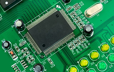
A PCB stackup is the arrangement of alternating layers of conductive copper and insulating materials within a printed circuit board (PCB). This layered structure is fundamental to the PCB's electrical and physical performance, impacting signal integrity, power distribution, and managing heat management.
An optimized PCB stackup design ensures efficient power delivery, maintains signal integrity, reduces electromagnetic interference (EMI), and enhances the overall reliability of the PCB. Conversely, poor stackup planning can lead to significant issues such as signal degradation, overheating, and compromised circuit performance.
Why is the PCB Stack-up Important?
The PCB stack-up plays a critical role in determining the overall performance and reliability of a circuit board. Here’s why it’s so important:
- Determines the Board’s Electrical Performance: A well-structured PCB stackup ensures efficient power and signal distribution across the board. By optimizing the path from the power source to the various components, the stackup minimizes issues like parasitic capacitance and inductance, which can degrade the board's performance. This optimization not only boosts the speed at which signals travel but also enhances the power delivery to various parts of the circuit.
- Influences Signal Integrity and Reduces Noise: Just like static on a radio disrupts the sound, electronic noise can interfere with the signals on a PCB, leading to errors and malfunctioning. A strategic PCB stackup design can mitigate this noise. By spacing out the conductive traces appropriately or segregating the analog and digital portions of the circuit, the design minimizes interference. Additionally, selecting materials with a low dielectric constant for the insulating layers can further reduce noise, ensuring cleaner signal transmission.
- Affects Electromagnetic Compatibility (EMC) and Reduces Emissions: For a PCB to function smoothly without affecting or being affected by external electronic devices, it must comply with EMC standards. A thoughtfully designed PCB stackup addresses EMC by incorporating features like adequate shielding, proper impedance matching, and optimal trace spacing. These elements help in minimizing electromagnetic emissions and susceptibility, thereby preventing the PCB from interfering with other electronic systems.
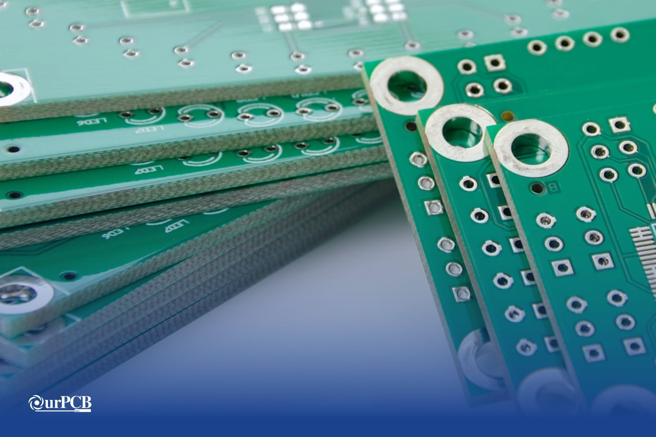
PCB Stackup Requirements
Foil Construction vs. Cap Construction
Foil is better than cap because it enables easier manufacturability with a better yield. The process also requires less core substrate material, which lowers the fabrication cost.
Cap construction is only recommended for hybrid circuit boards that have specialty laminates. You can also use this process if the PCB has blind vias and you don’t have the required drilling tools, like laser drills.
Board Component Density (Number of Layers and Spacing)
A board’s component density is one of the most common drivers for multilayering. Each component requires at least two traces to break out its signals, so the more they are, the more traces are required inside the board, which might require several copper layers.
High pin count processors or packages like BGA complicate the stack further, because each one requires multiple traces to break out their signals. If the board has several of these components, its stackup must accommodate the wiring for all these incoming and outgoing signals.
What Materials are Used in PCB Stackups?
Copper for Conductive Layers
Copper is the material of choice for signal traces, as well as power and ground planes. Power and ground planes are wider copper surfaces that supply power or provide a low-resistance return path, respectively.
Prepreg and Core for Insulation
The PCB core is a hardened and cured material that provides structural support. It also insulates two adjacent copper layers in dual or multilayer boards. Some multilayer boards can have two or more core layers to enhance the structural integrity. A typical example of core material is FR4.
Prepregs only provide insulation. These dielectric materials are usually sandwiched between two cores or between the core and the copper foil.
Special Materials for High Frequency Applications
Materials like Rogers, Isola, and DuPont are ideal core/substrate materials for high-frequency PCB construction because they have a low dielectric constant and loss.
What are the Challenges in PCB Stackup Design?
Managing Cross-Talk Between Closely Packed Traces
The closely packed PCB stack in high-density circuits has thin insulations between the layers. This stackup increases the chances of cross-talk. But it’s possible to avoid this issue by optimizing the trace routing and arranging the layers in an alternating pattern between ground and signal.
Ensuring Impedance Control Across All Layers
Impedance matching is more challenging in high-frequency multilayer circuits. But modifying the stackup arrangement and prepreg thickness can ensure better impedance control. Materials like PTFE enable more precise impedance matching between the signal layers because they have a low dielectric constant and loss.
Balancing Thermal Management With Electrical Performance
A material like ceramic provides the best thermal management, but its electrical performance, specifically impedance matching, is not the best.
Special Offer: Get $100 off your order!
Email [email protected] to get started!
How does Layer Count Affect PCB Stackup?
More Layers can Improve Signal Integrity
Increasing the layer count to have dedicated power and ground planes improves signal integrity. In RF PCBs, the ground plane should be adjacent to the signal layer to provide the shortest return path.
Higher Layer Count Increases Manufacturing Costs
The more layers in the stack, the higher the cost of the board. These extra layers jack up the price in two ways. First, there are the extra materials needed to fabricate them. Second, there are the additional manufacturing and labor costs associated with processes like etching, lamination, and hole drilling.
Complexity in Design and Testing Increases
Designing a multilayer PCB is a complex process that requires keen attention to detail. After passing DFM, DFA, and DFT checks, manufacturing is more complicated, and so is the testing process. Therefore, the lead time will be longer.
Steps to Build PCB Stackup
Determine the Number of Layers
- Decide how many layers are necessary based on the circuit complexity, signal integrity needs, and budget. Assess the needs for power distribution, signal routing, and electromagnetic compatibility (EMC) to choose an appropriate number of layers.
Choose Layer Materials
- Select materials that will impact the PCB's performance, durability, and manufacturability. Common materials include FR-4 for general purposes, high-speed laminates for improved signal integrity, and metal cores for better heat dissipation.
Define Layer Functions
- Assign specific functions to each layer, such as signal, ground, or power. Plan to optimize signal integrity and minimize cross-talk and interference, often using inner layers for power and ground planes to shield and reduce electromagnetic interference.
Configure Layer Thickness
- Determine each layer's thickness to control impedance and support component assembly. Typical copper layer thickness ranges from 1 oz/ft² to 2 oz/ft², depending on required impedance characteristics and physical strength.
Plan Impedance Matching
- Match impedance across traces and layers to ensure signal integrity. Use PCB design software to calculate the needed impedance based on trace width, spacing, and dielectric material, adjusting the layer configuration as necessary.
Integrate Via Structures
- Connect layers electrically using vias. Choose between through-hole, blind, and buried vias based on the board layout's complexity and density, ensuring via placement does not disrupt critical signal paths.
Design Layer Stackup
- Create a visual stackup diagram using PCB design software, showing the types, thicknesses, and functions of each layer, helping to visualize and finalize the arrangement of layers.
Thermal Management Planning
- Address heat distribution and dissipation. Incorporate thermal vias and consider heat sinks or thermal relief pads, especially near heat-generating components.
Review and Optimize
- Conduct reviews with design and manufacturing teams to ensure the stackup and overall PCB design are optimized for functionality, manufacturability, and cost-efficiency.
Prototype and Test
- Produce a prototype board and perform testing to evaluate electrical performance, thermal management, and mechanical stability. Iterate on the design based on test results to refine the board before full-scale production.
Common Types of PCB Stackups
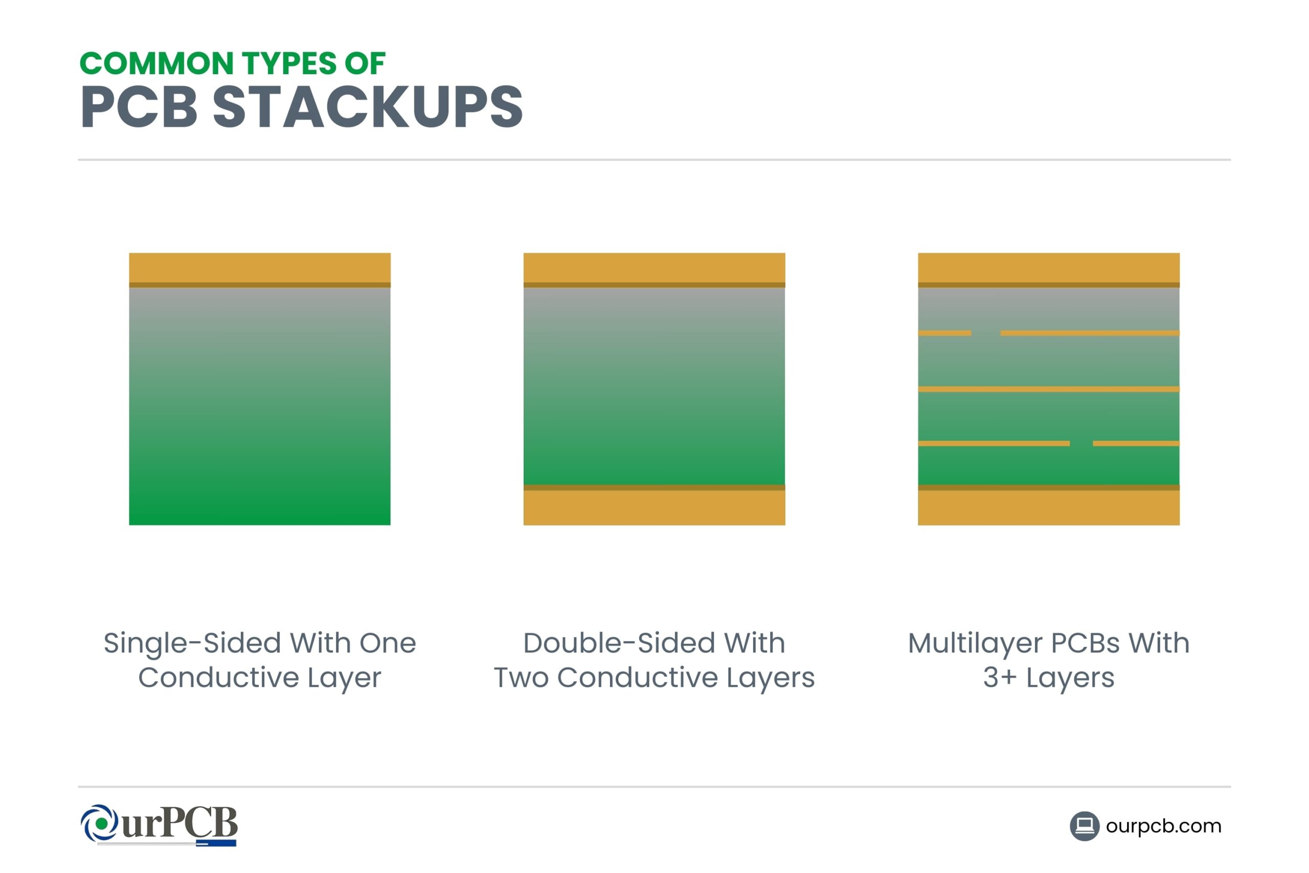
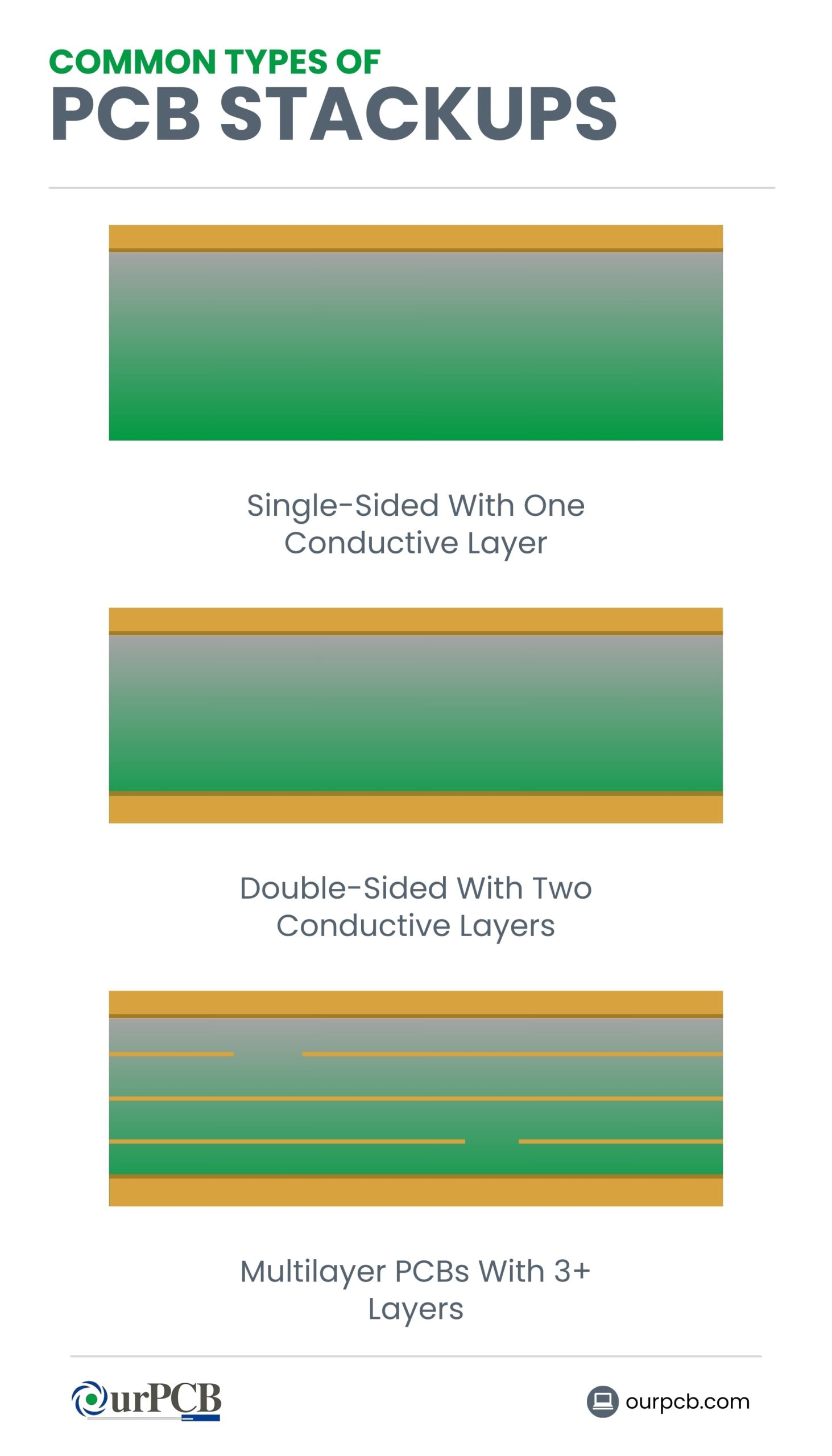
Single-Sided With One Conductive Layer
These are the simplest PCBs because they have only one copper layer with the components mounted on one side.
Double-Sided With Two Conductive Layers
The two conductive layers in this board stackup provide twice as much routing space as a single-sided PCB of the same size. This kind of board also has components mounted on both sides. It’s still relatively easy to design.
Multilayer PCBs with 3+ Layers
These boards have the most complex stackup designs because they have at least three copper layers. As the layer count goes up, the PCB's design becomes more complex, and the cost increases. Design-wise, you have to consider factors like signal integrity, impedance matching, and noise when creating the stack.
Common Types of PCB Layer Stackups

PCB layers
2-Layer PCBs
2-layer boards have one copper layer on each side of the substrate. This simple design is ideal for non-complex devices like power supplies, HVAC, power conversion systems, and scientific calculators.
4-Layer PCBs
These PCBs add on two internal dedicated planes for the power and ground. Their primary use is in power electronics with small digital sections. Complex industrial systems also rely on this 4-layer stack PCB.

An example of a 4-layer PCB stack up
6-Layer PCBs
A 6-layer PCB is equivalent to a 4-layer board with two extra signal layers. This board is common in advanced communication equipment.

An example of a 6-layer PCB stack up
8-Layer PCBs
8-layer circuit boards have two additional signal layers added to a 6-layer board, which provides more routing flexibility. This design also makes it possible to have a dense circuit. Typical applications include telecommunication equipment and high-speed computing devices.
An example of an 8-layer pcb stack up
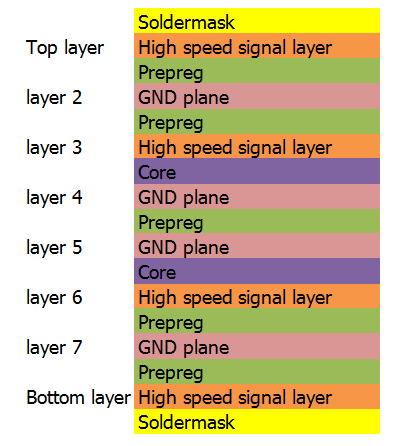
10-Layer PCBs
A 10-layer stack has alternating signal and ground layers in the outer four layers to prevent interference. The two innermost copper planes provide power, one for each side. This arrangement creates complex boards for applications like GPS devices and internet servers.
How is a PCB Stackup Designed?
Considering Signal and Power Integrity Early
PCBs pack large circuits into a thin stack, which exposes the signal and power lines to interference, especially in multilayer designs. Planning the design early is critical to prevent issues like signal degradation and interference.
For instance, in a 10-layer PCB, the outer 4 layers on each side alternate between signal and ground. This design creates noise-canceling barriers between the signal lines. The top and bottom layers should also be signal traces to mount the components.
Besides proper layer arrangement, other factors like via placement, via plugging, and separating the grounds for analog and digital sections ensure the board has signal and power integrity.
Balancing Cost and Performance for Efficiency
Reducing the copper layer count and using cost-effective materials for the core and prepreg will keep costs low. However, these cost-cutting measures can harm performance.
In a PCB with digital and analog components, for example, the stack should have at least two ground planes for these two component categories. The insulating layers are equally as important, especially in high-speed, high-frequency PCBs.
A core material like Rogers is better for such circuit boards, but it’s costlier than FR4. You have to balance between these two factors when developing the stack.
Selecting Appropriate Materials for Specific Applications
Copper is the standard material for the power, signal, and ground layers. What changes is the core material, and FR4 is the most common because it’s affordable.
But it has its limitations. FR4 is not ideal for circuits with multiple LEDs because it can’t dissipate the heat efficiently. In high-temperature cases, aluminum or ceramic makes the best core material.
PTFE materials (Teflon) provide stable dielectric properties at higher CTEs, making them ideal for high-speed, high-frequency applications. Rogers is a ceramic-filled PTFE, which makes it more stable than regular PTFE, but more costly as well.
What Factors Influence PCB Stackup Design?
Number of Layers Based on Complexity
Complex circuits require more layers because it’s necessary to separate the traces to accommodate the complex routing. Increasing the layers also makes it possible to have a high-density design, increasing the functionality and capability of the board. Vias interconnect the copper layers in the stack, and you can use via-in-pads to save on space.
Type of Signal (Digital or Analog) Being Used
Analog components are more susceptible to noise due to their operation in the linear regime. The stack should have separate ground planes for the high-and low-frequency analog signals. To maintain a consistent ground potential throughout the system, you can use stitched vias to interconnect these ground planes separately.

PCB vias
However, digital components operate at saturation, meaning only high noise levels can cause interference. These parts don’t require separate ground planes for high-frequency and low-frequency signals.
Impedance Requirements for Signal Integrity
Consider these factors for impedance matching:
- Trace geometry
- Spacing between the signal trace and its return path
- Dielectric material (core and prepreg)
PCB Stackup FAQs
How do Power/Ground Planes Function in PCB Stackups?
Power and ground planes are dedicated copper layers in the PCB stackup that distribute power and provide a low-impedance return path. These return paths help reduce EMI by channeling the disturbance outside the circuit.
How does Plane Decoupling Help in PCB Stackup Design?
Plane decoupling is a technique that uses decoupling capacitors near power and ground plane pairs to provide clean power to noise-sensitive components.
How do EMI/EMC Considerations Affect PCB Stackup Design?
EMI/EMC considerations lead to careful placement of signal, power, and ground planes. The stack can even have shielding layers.
Back to top: What is a PCB Stackup?
Special Offer: Get $100 off your order!
Email [email protected] to get started!