When developing an electronic circuit, you will want to protect it against electromagnetic interference. Otherwise, it will experience unusual problems, leading to performance degradation and failure. Not only that, but it may also affect other sensitive electronics due to signal leakage. For this reason, we recommend installing PCB assembly manufacturers circuit shields onto your system. This technology ensures circuit board longevity and safety while also blocking electromagnetic radiation.
By reading this article, you will understand the benefits of PCB shielding and the types available on the market. So let’s get started!
Contents
- What is EMC Shielding?
- Consequences of unshielded electronics
- Implementing EMI Shielding in Your PCB Layout
- Shielding at the Lowest Possible Levels
- Attenuates Noise Between Chips
- Protects Analog and Digital Components From Wireless Module Noise
- Enables Uncompromised Connections
- Low Cost and Lightweight
- Traditional PCB Shielding Techniques
- PCB Shielding Metal Cans
- PCB Shielding Frames and Covers
- Types of PCB Shielding
- PCB RF Shielding
- Arduino Shielding
- Why Are Arduino Shields Better than Others?
- The typical features of PCB level shield cans
- PCB Shielding Can vs. EMI Shielding Can: What Is the Difference?
- Typical Shielding Materials
- Typically, shielding comes with the following materials:
- Typical Shortcomings of Traditional PCB Level Shielding Techniques
- Consume Space
- Difficult to Inspect, Rework, or Remove
- Not Flexible
- Application Areas of EMI PCB Shields
- FAQs
- How Do You Shield a Circuit Board?
- How Thick Is PCB Shielding?
- How Do You Shield PCB Traces?
- Summary
What is EMC Shielding?
 RF shielding enclosure
Electromagnetic Compatibility (EMC) shielding generally involves protecting sensitive signals against outside electromagnetic signals.
It also helps to ensure that stronger signals cannot escape, which could disrupt neighboring devices.
In this case, electromagnetic frequencies may produce a communication line or interrupt a safety-critical signal.
Overall, this safeguard will work with ICs, sensitive components, and wires connected to each PCB.
As a result, circuits designed with this technology will prevent signal disruption via the shielding features.
Consequences of unshielded electronics

Unshielded electronics may eventually disrupt wireless devices.
Interference such as crosstalk, power supply noises, and ground bounce can significantly affect electronics, leading to performance issues.
However, electromagnetic interference (EMI) poses a more significant threat because it can devastate an electronic device’s functionality.
Not only that, but it may also result in catastrophic and expensive consequences.
For example, EMIs can also cause medical devices to fail, resulting in dire consequences.
If you fail to control the EMI in an electronic device, the following problems may arise.
- Communication disruptions
- Interference with wireless devices
- Results in corrupted sensor data
- Electronic component failure
- Software errors or defects
 Electromagnetic interference can corrupt sensor data.
A poor circuit board layout will usually produce electromagnetic interference.
Unsolved issues relating to the generated EMI will result in poor board performance, causing it to eventually malfunction.
You can prevent this from happening by improving PCB design techniques.
Implementing EMI Shielding in Your PCB Layout
A PCB layout may feature any shielding material.
Electromagnetic shielding materials exist on the market, many of which provide practical and straightforward solutions. Sometimes traditional methods involving filters and best layout practices may not work as expected. In that case, you should mount any of these mechanisms in your PCB layout:
- Metal shielding cans: You can wrap a custom-made metal shield (metal box) around noise-generated circuits to restrict excessive electromagnetic radiation.
- Elastomer electromagnetic shielding materials: This material on specific components and connectors will help limit electromagnetic radiation.
- Ferrite beads, rods, and plates: If traditional filter circuits malfunction, then ferrite beads, rods, and leaves can work like an EMI filter.
- High conductivity mesh materials: Rather than rigid shielding cans, you can install mesh materials, Ideal for flexible or rigid-flex boards.
- Separated/star ground replacements: Uniform ground planes will supply several grounding points. Plus, you can easily ground conductive shielding materials.
You will also need to follow best practices when installing the shielding to your PCB layout. Doing so will allow your design to pass EMC tests.
Shielding at the Lowest Possible Levels
The lowest levels in terms of shielding refer to the individual chips and tiny sections of the PCB. This shielding has several benefits that positively impact the board’s performance.
Attenuates Noise Between Chips
Shielding helps attenuate interference between the individual chips mounted on the board. It also provides better noise cancellation at higher frequencies in the gigahertz range.
Additionally, chips are becoming smaller and have faster rise times with lower noise margins. These designs require PCB-level shielding to keep out electromagnetic interference.
Protects Analog and Digital Components From Wireless Module Noise
Electronic products also increasingly incorporate wireless modules like Bluetooth and Wi-Fi into the circuits, which introduces a lot of interference to the nearby analog and digital components. Enclosure shielding is not as effective at preventing this noise, but PCB-level shielding can work.
Enables Uncompromised Connections
Plus, circuit boards must have access slots and holes for the I/O cables, heat ventilation, display cables, etc. These holes will compromise enclosure shielding.
Even if you filter all the cables, you won’t be able to keep out all the noise. This makes low-level PCB shielding the most viable option.
Low Cost and Lightweight
And when you look at it from the cost and weight perspectives, shielding at the lowest PCB level is cheaper and lighter than enclosure shielding.
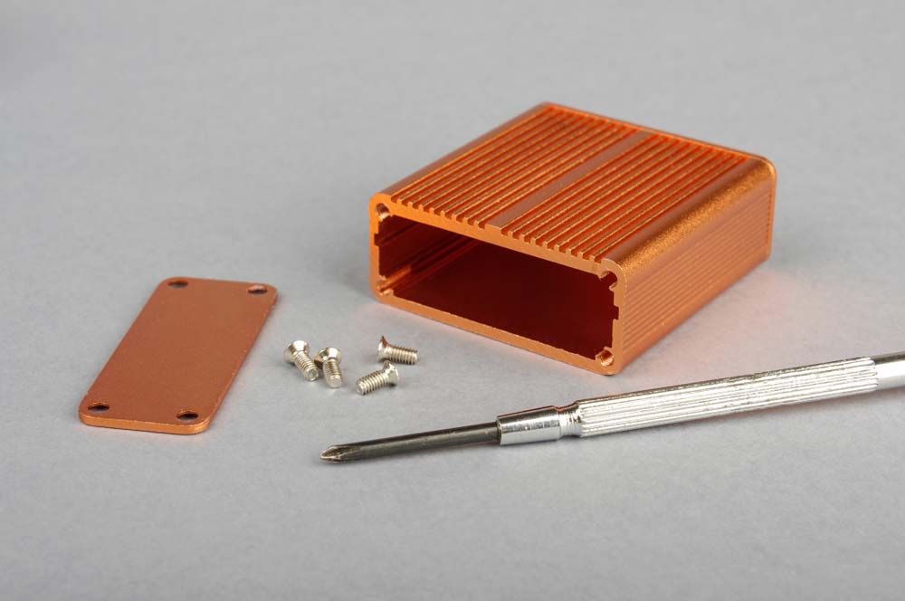
An aluminum enclosure for circuit boards
Traditional PCB Shielding Techniques
PCB designers, manufacturers, and assemblers traditionally relied on metal cans, frames, and covers to shield circuit boards.
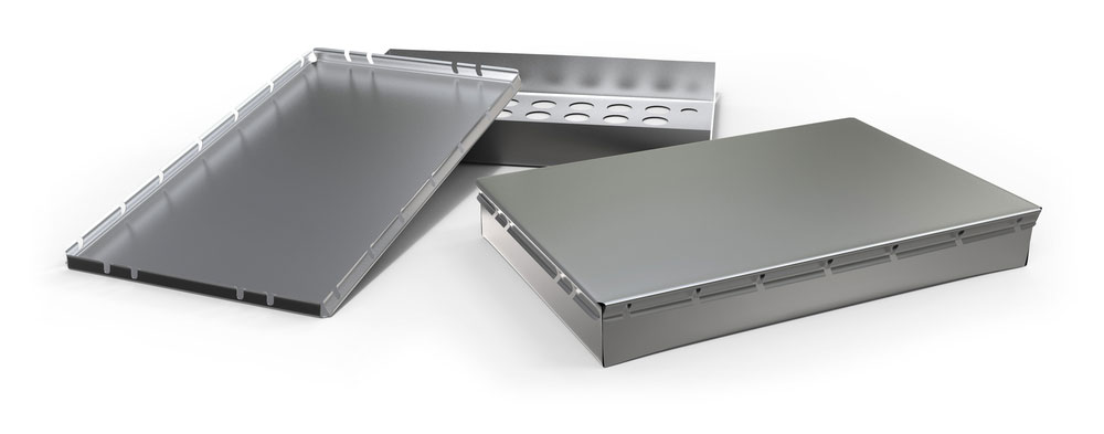
PCB Shielding Metal Cans
These shields resemble the metal cans you use to store sensitive items and assemblers mounted them directly onto the PCB during the reflow process.
Some installed these shields after the reflow process using tiny clips that they instead solder to the PCB during reflow.
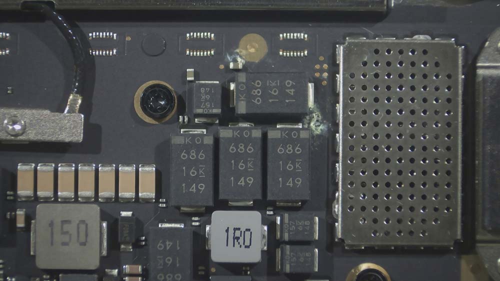
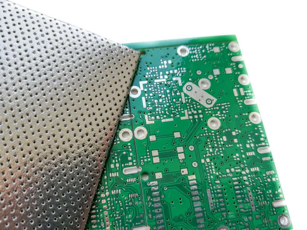
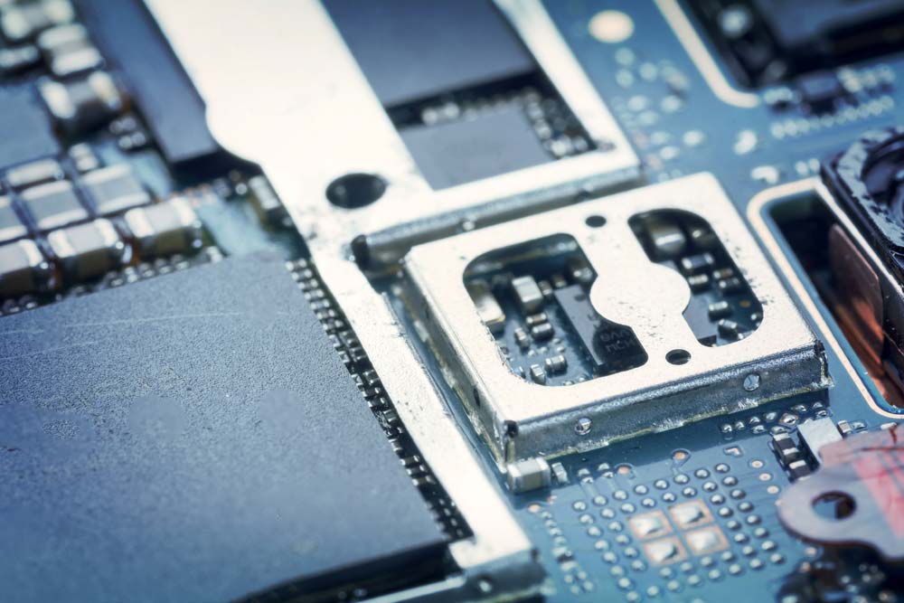
An EMI shield on a logic board
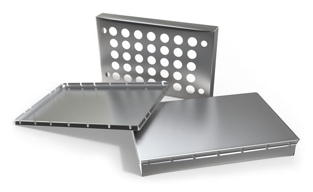
PCB Shielding Frames and Covers
Frames also sit firmly on the PCB after being soldered during or after reflow, after which the cover snaps into them to shield the component(s).
A close-up image of the frame and cover PCB shields
Special Offer: Get $100 off your order!
Email [email protected] to get started!
Types of PCB Shielding
Two main PCB shielding types exist today: PCB RF shielding and Arduino shielding.
-
PCB RF Shielding
RF shielding blocks electromagnetic radiation and radio frequencies by lowering the coupling of electromagnetic fields, electrostatic, and radio waves. These shields may also feature a Faraday cage, which impedes electrostatic fields.
RF shielding enclosure
-
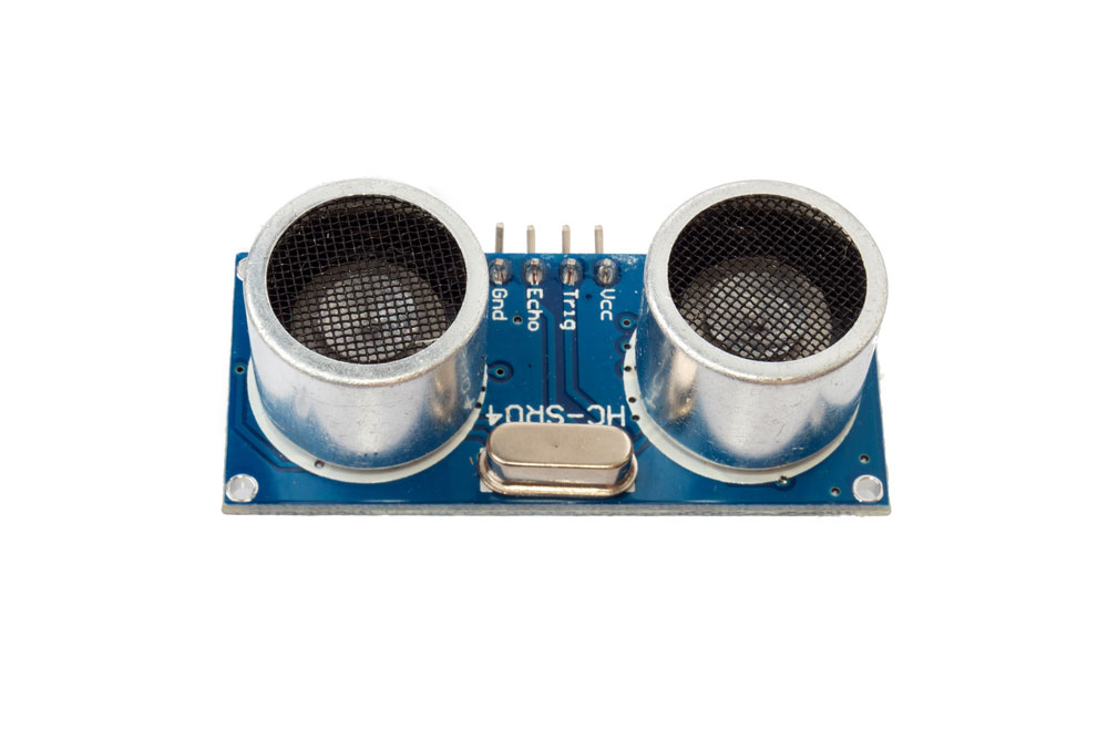
Arduino Shielding
Arduino’s EMI PCB shield features shield pins down the sides, allowing you to mount it atop an Arduino PCB. As a result, the circuit’s functionality will increase.
More importantly, you should also pay special attention to any reserved pins.
If a sensor utilizes the I2C or SPI bus, it cannot operate as the input and output on another shield. You can purchase a wide selection of securities from Arduino.
-
Why Are Arduino Shields Better than Others?
Overall, an Arduino shield is easier to handle and cost-friendly than other types. It also features a library with sample, editable code, allowing you to develop and assemble a project. Plus, you can stack a shield board atop an Arduino, creating a complete system.
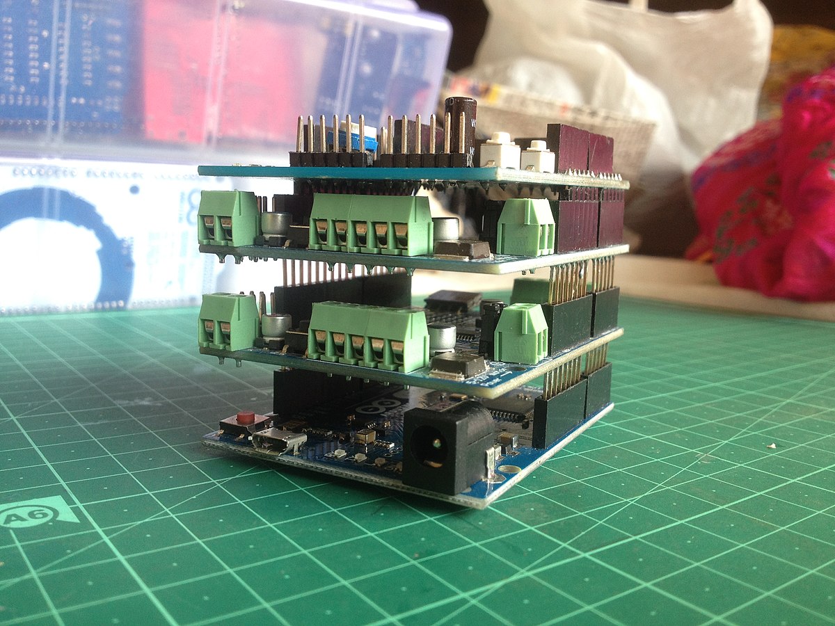
Arduino shield boards stacked atop each other.
Source: Wikimedia Commons
The typical features of PCB level shield cans
A PCB level shield typically offers the following features in its design:
- Small footprints
- Low-profile configurations
- Two-piece security: fence and cover
- Through-hole or surface mount
- Multi-cavity patterns
- Unlimited design possibilities
- I/O holes
- Connector cutouts
- Ventilation holes
- Removable covers to easily access components
- Extended shielding with RF absorbers
- Secure locking mechanisms to protect against shock and vibration
- ESD protection featuring insulation padding
PCB Shielding Can vs. EMI Shielding Can: What Is the Difference?
The difference between the two lies in the scope and application. PCB shielding can operate on the localized level, where they create Faraday cages to isolate and enclose circuits, while EMI shielding can provide globalized shielding.
Since localized shielding is more effective in modern-day electronics, PCB shielding cans are better than EMI shielding cans. However, some applications demand EMI shielding cans, so the choice between the two depends on the application.
Typical Shielding Materials
Electronic PCB shielding material for electromagnetic compatibility solutions.
Typically, shielding comes with the following materials:
- Tin plated cold rolled steel
- Tin plated copper
- Nickel silver
- Stainless steel
- Tin plated phosphorous bronze
We recommend selecting the tin-plated steel if you need to shield below 100 MHz on a circuit. Meanwhile, tin-plated copper will protect against ratings higher than 200 MHz for your printed circuit board.
Tin plating makes it easier to solder the shield. On the other hand, aluminum has heat-sinking properties, so it cannot shield it.
Typical Shortcomings of Traditional PCB Level Shielding Techniques
Although effective at keeping out the noise, traditional PCB-level shields are not perfect.
Consume Space
The first thing you’ll notice when you look at them is they consume a lot of space, which is a precious commodity on compact boards. They also make the PCB heavier.
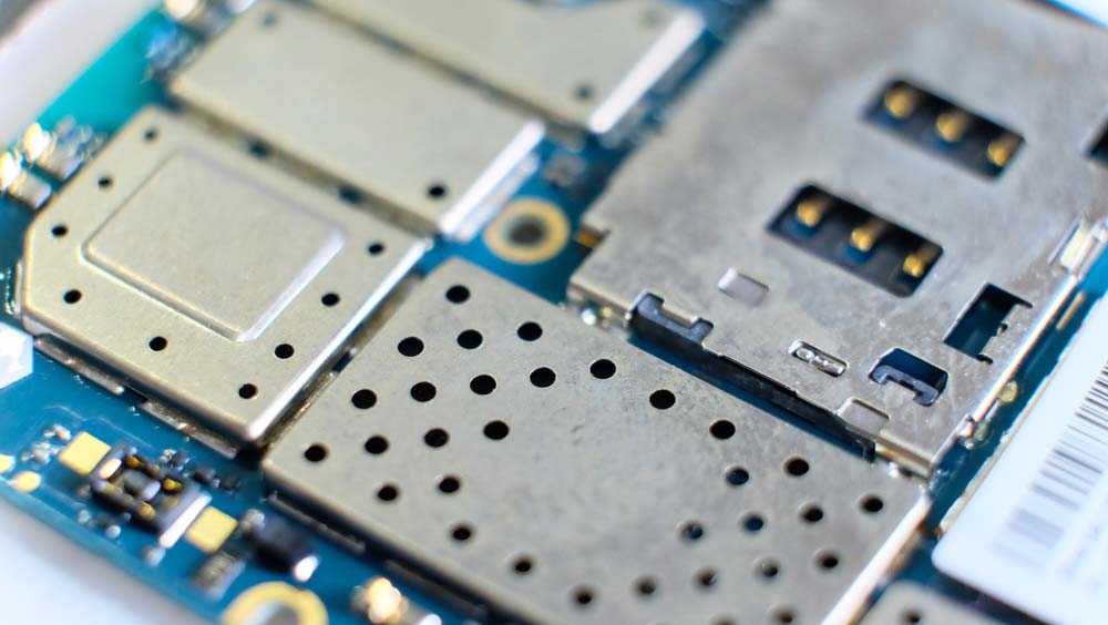
A mobile phone PCB with several low-level metal shields
Difficult to Inspect, Rework, or Remove
Should any malfunction occur, these components are difficult to inspect, rework, and remove. Remember, the can (clip) or frame must be soldered to the PCB.
Not Flexible
You cannot use these shields on flexible PCBs or areas requiring flexible movement.
Application Areas of EMI PCB Shields
PCB EMI shields are common in consumer electronics like smartphones, medical equipment like MRI machines, avionics systems, networking devices, automotive electronics like head units, industrial automation devices, and energy systems.
FAQs
How Do You Shield a Circuit Board?
You shield the circuit board by installing the selected material using a conductive adhesive tape, soldering it directly to the PCB, or soldering clips, clamps, or frames to hold the shield, which you’ll snap into place.
How Thick Is PCB Shielding?
The standard thickness is 0.12mm for copper and tin shields, but there is the option of 0.18mm for both or tinned steel at a 0.2mm thickness.
How Do You Shield PCB Traces?
Shielding individual traces is a little tricky because they are tiny, but you can use mesh screens, conductive foils, or paint to isolate and secure them from external noise.
Summary
Overall, PCB shields provide the necessary protection for your custom circuits. Of course, you will need to ensure that the circuit meets the criteria. It achieves this through specially designed material that works best for a specific frequency range. For example, you can utilize tin-plated steel for a device below the 100 MHz ratings. Additionally, RF shields help to block out radio frequencies and electromagnetic radiation. At the same time, other affordable options exist on the market today, especially the Arduino boards.
Do you have any questions regarding PCB shields? Feel free to contact us!
Special Offer: Get $100 off your order!
Email [email protected] to get started!