Every printed circuit board has a specific function for different applications and electronic devices. Most of these electronic applications require high thermal expansion properties. One PCB that offers lesser signal loss and higher frequency distribution is the 10-layer PCB fabrication.
A 10-layer Pcb fabrication is done such that when all PCB layers are combined, the board thickness and size is 3.2mm at max. This method allows the board to offer better flexibility and signal integrity when used.
Contents
- What is a 10-layer PCB?
- What is 10 Layer PCB Stack Up?
- What Is a Standard 10-Layer PCB Stack Up?
- Thickness of a 10-Layer PCB Stack Up
- Copper Thickness of a 10-layer PCB Stackup
- Glass Transition Temperature of a 10-Layer PCB Stack-Up
- What are the Applications of a 10-layer PCB?
- Computer and consumer electronics industry
- Telecommunications Industry
- Industrial Processing Industry
- Medical Equipment Industry
- Military and Defense Industry:
- Automotive Industry
- Aviation and Aerospace Industry
- How Do You Pair Signal Layers on 10-Layer PCB Stack-Up
- Factors That Determine the Designs of a 10-Layer PCB Stack-Up
- Design and Production Costs
- Application Area
- Design Configuration
- Electrical Specifications
- Component Density
- What is the 10-layer PCB manufacturing process?
- Advantages and disadvantages of 10 Layer PCB
- 10-layer PCB Advantages
- 10-Layer PCB disadvantages
- 10 Layer PCB materials
- 10-Layer PCB Stack Up Storage Conditions
- How Do You Test the 10-Layer PCB Stack Up
- How to select a 10-Layer PCB Manufacturer?
- Production costs
- Design techniques
- Perfect production equipment
- Storage Condition Used
- The time of delivery
- Minimum order quantity
- The price
- Customer service
- Conclusion
What is a 10-layer PCB?
The 10-layers PCB is a multi-layer printed circuit board made of conductive material. Generally, the 10-layer PCB is most common in electronic devices requiring high electromagnetic conductivity. It is essential in integrated circuits needing multiple close routing of high-speed signals.
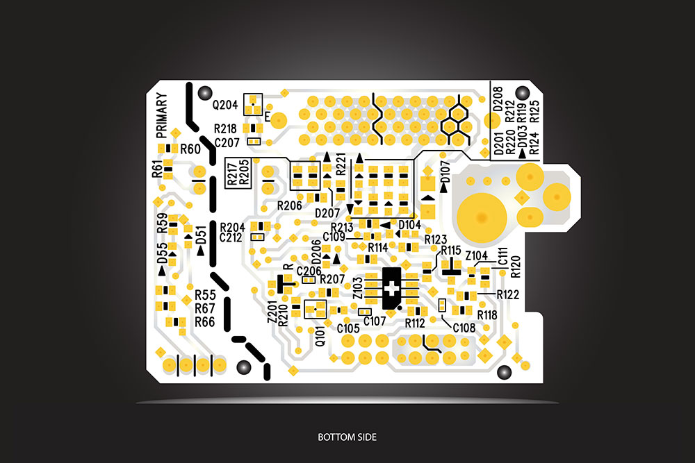
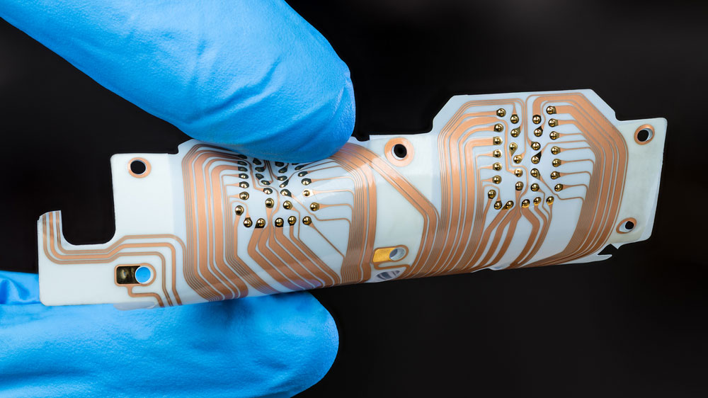
(The bottom of a 10-layer printed circuit board).
What is 10 Layer PCB Stack Up?
A 10-layer is the insulator and copper layout arrangement before coupling the printed circuit board. Usually, the board layers comprise vital parameters such as signal layers, power planes, copper weights, pad spacing, drill hole sizes, trace widths, etc.
Getting your 10-layer stack-up gives you an idea of the PCB design and behavior before it is complete. Further, the stack-up board size helps determine the signal loss in the internal layers of the printed circuit board.
What Is a Standard 10-Layer PCB Stack Up?
The thickest layer in a PCB stack is the core or substrate, which insulates the inner copper layers from each other and the prepreg. This core’s thickness can vary, going to lows of 150 μm and highs of 300 μm.
The standard substrate thickness is 200 μm because this separation meets the insulation requirements for general-purpose circuit boards. The copper layer’s thickness is usually standard at 18 μm, but the prepreg can either be 80 or 125 μm.
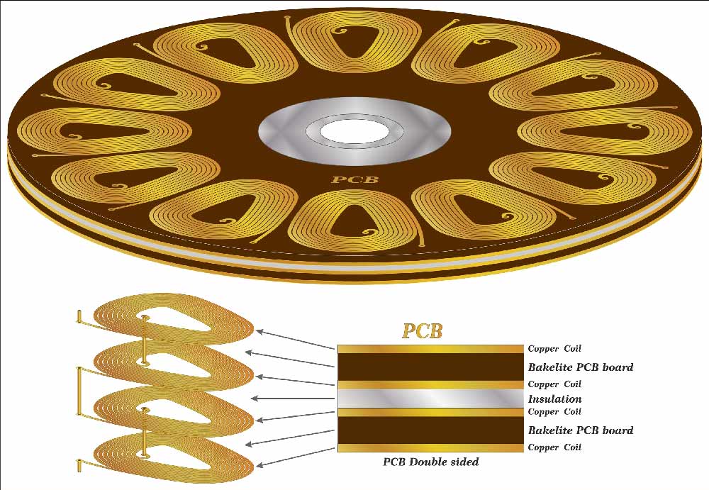
The multilayer PCB stack of a three-phase stator
Thickness of a 10-Layer PCB Stack Up
The thickness of a 10-layer PCB varies from 1.33 to 3 mm depending on the core and prepreg thickness variations.
Copper trace thicknesses can also vary but are usually standard at 18 μm.
For instance, if the traces are meant to handle high current levels, they can be as thick as 105 μm.
Some 10-layer boards that require more isolation between the conductive lines can also have double simultaneous prepreg layers.
If you have the maximum values for each layer, the board can be pretty thick.
Generally, FR4 boards with more than 6 layers must have thinner laminates to manage the overall thickness of the PCB.
Combinedly, these layers should be 0.8 to 1.2 mm thick (800 - 1200 μm), but they can be 1.6mm in under-6-layer boards because they have fewer copper and prepreg layers.
Copper Thickness of a 10-layer PCB Stackup
The copper foil forms the electrically conductive layer in the PCB, and if the board transmits high electrical current, it can be as thick as 3 ounces (105 μm).
Thick traces are also necessary for efficient heat transmission from the inner layers to the outside. Therefore, if the transmission lines or components generate a lot of heat, the board must have thick traces to channel the heat outside, usually through via-holes.
Glass Transition Temperature of a 10-Layer PCB Stack-Up
Considering most industry standards require lead-free soldering for environmental safety, the glass transition temperature should be over 170°C for 10-layer boards to ensure maximum reliability.
What are the Applications of a 10-layer PCB?
The main aim of a 10-layer printed circuit board is to cut down signal loss, as seen in ball grid arrays. Hence, the following industries are famous for their applications of this multi-layer PCB.
Computer and consumer electronics industry
Most computer electronics consist of the 10-layer printed circuit board. Meanwhile, some electronic devices use ball grid array technology for better thermal dissipation, frequency transmission, conductivity, etc.

(Some consumer electronics).
Telecommunications Industry
This industry also has a massive application for the 10-layer printed circuit board. It requires signal transmission over long distances. As a result, telecommunications need circuit boards with high thermal expansion and high-frequency information.
Industrial Processing Industry
Like the others, the 10-layer printed circuit board is important in industrial processing for its heat dissipation properties. Also, reduced signal loss is an essential quality of 10-layer boards in the processing industry.
Medical Equipment Industry
Digital medical equipment functions by transmitting low-frequency and high-frequency signals. Also, a low signal loss found using 10-layer PCBs is crucial for better readings.

(Most medical equipment utilizes 10-layer PCBs for accurate readings)
Military and Defense Industry:
The military sector uses 10-layer printed circuit boards the most. Since all military equipment, weapons, and machinery relies on accurate data and readings, these multi-layer boards have become more critical.
Automotive Industry
The automotive sector also needs multi-layer boards with optimal thermal expansion without signal loss. Therefore, 10-layer printed circuit boards are the best option in this case.
Aviation and Aerospace Industry
The primary PCBs used in the aviation and aerospace industry is 10-layer types. It is because they offer better signal transfer for satellite communications.
How Do You Pair Signal Layers on 10-Layer PCB Stack-Up
10-layer circuit boards have six signal layers, and you must take care of how you arrange them to ensure the best transmission performance with minimal losses.
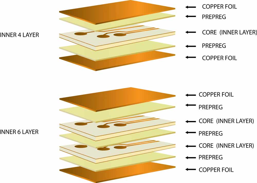
Inner 4-& 6-layer stacks in multilayer PCB
An example is pairing two outer layers (one and ten) to transmit low-frequency signals while three and four handle high-speed signals.
Use the seventh and eighth layers to transmit high-speed, high-frequency signals, as well.
This leaves layers two, five, six, and nine as the plane layers for powering, grounding, and protecting the signal layers.
You can use two and nine to protect high-frequency signals from their low-frequency counterparts while the ground and power planes sit in the middle.
This separation of the high-frequency, high-speed sides will reduce noise interference.
Factors That Determine the Designs of a 10-Layer PCB Stack-Up
Design and Production Costs
Some unique or complex 10-layer PCBs require specific electrical requirements to function, which means they require more time, expertise, and machinery during fabrication. These additions cost more, so designers try to keep the PCB design as simple as possible or closely match the standard designs to lower production costs.

Engineers in an electronics production plant designing PCBs
Application Area
Different application areas require different PCB requirements or specifications. For instance, 10-layer PCBs built for telecommunication applications require extra shielding to keep the signal lines free from interference. On the other hand, those designed to run in an electromagnetic environment must have high electromagnetic compatibility. These features come about in the design phase.
Design Configuration
Circuit boards are usually part of a bigger design or module, so their designs should follow the conditions in the larger plan. For instance, if the module has limited space, the 10-layer board can have flexible interconnecting sections, meaning you’ll have two interconnected 10-layer PCBs.
Electrical Specifications
Boards can have different electrical specifications that you must factor into the design. Think of things like heat dissipation, signal integrity (in high-frequency applications), electromagnetic compatibility, etc. These factors affect the trace routing style and how thick the PCB should be, which you must incorporate into the design.
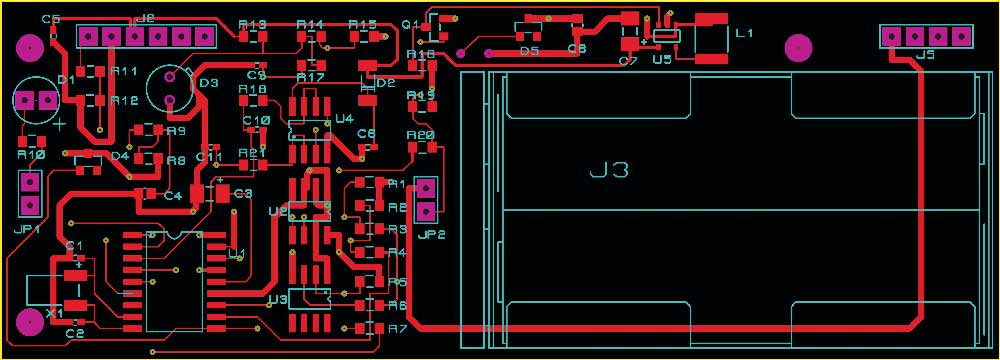
Trace routing in a multilayer PCB during the design phase
Component Density
If the PCB will have dense components, you have to manage the trace designs and the space available to mount them with minimal signal interference. And since you’re dealing with a 10-layer board, this is most likely the scenario. Some design tips include avoiding long, parallel trace placements in the same layer. Utilize the multiple layers to break the signal lines, which will prevent electrical issues.
Special Offer: Get $100 off your order!
Email [email protected] to get started!
What is the 10-layer PCB manufacturing process?
The 10-layer PCB manufacturing steps are as follows:
- Create the intended PCB design.
- Transfer the prototype to a board.
- Ensure the right copper thickness by carefully etching it to the sheet layer.
- Apply the silkscreen and solder mask.
- Couple the integrated circuit components.
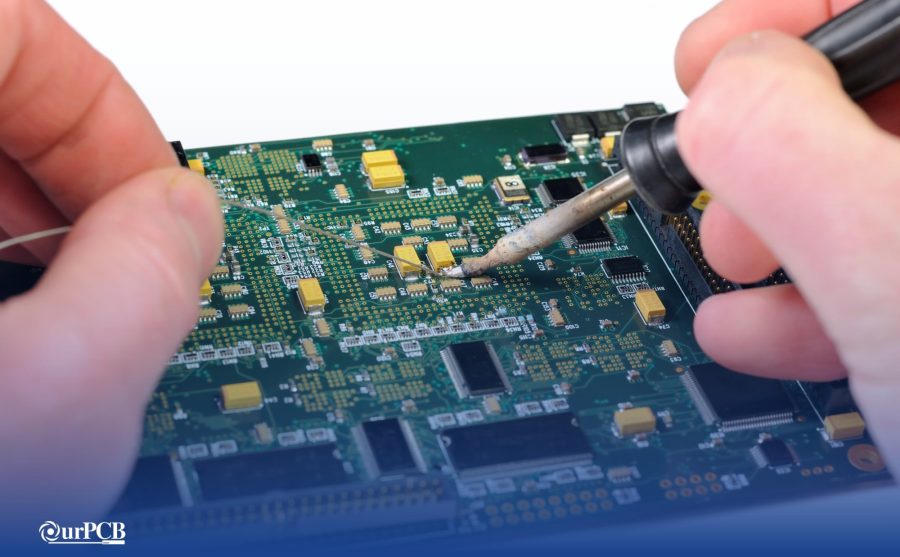
- Lastly, test the finished circuit board.
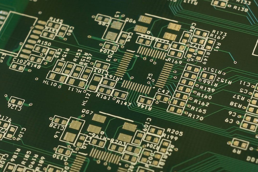
(A finished multi-layer printed circuit board).
Advantages and disadvantages of 10 Layer PCB
10-layer PCB Advantages
Here are some reasons 10-layer PCB stack-ups make an excellent choice.
- It is lightweight.
- The relative manufacturing cost is less than single-layer PCBs and two-layer PCBs.
- There is better flexibility.
- It guarantees better performance.
- It delivers high-speed signals due to the many layers of conductive material.
- There is increased power density.
10-Layer PCB disadvantages
On the other hand, 10-layer printed circuit boards are not perfect. Therefore, you should know the drawbacks before choosing to purchase one.
- The cost is high.
- It is not widely available.
- There is a higher chance of manufacturing defects.
- It requires specialized industrial control and handling.
- Design time is longer.
- Professionals with expertise in this design are required to build it.

(A female engineer working on a PCB)
10 Layer PCB materials
These materials contribute to the unique properties of a 10-layer printed circuit board. Some 10-layer PCB materials involved in the manufacturing process include:
- FR-40 dielectric material
- Copper layers
- Outer layers
- Ground layers
- Ground planes
- Silkscreen
- Solder mask
- Teflon substrate or Polyimide
(Copper Layer of a PCB)
10-Layer PCB Stack Up Storage Conditions
The two most important factors to avoid when storing a 10-layer PCB are electrostatic discharge and moisture. ESD is easier to keep at bay so you have to be keen about the moisture. First, place these boards in vacuum-sealed moisture barrier bags with a desiccant card or bag inside. Once sealed, place this package in a dry place with no sharp objects that can puncture the bag.
How Do You Test the 10-Layer PCB Stack Up
On a 10-layer PCB, you can perform several electrical and functional tests plus inspections, the most common one being ICT. In-circuit testing or bed-of-nails testing is the most accurate electrical and functional test, but it is expensive.
Another common electrical test is the flying probe method, a non-powered testing procedure that checks for open circuits, shorts, capacitance, resistance, diode issues, and inductance.
You can also use automated optical inspection (AOI), X-ray inspection, and burn-in testing to ensure the multilayer board is fully ready to use.
How to select a 10-Layer PCB Manufacturer?
Before choosing the proper multi-layer PCB manufacturer for your project, here are things to consider.
Production costs
Ensure the manufacturer has extensive capacity to handle your project. To an extent, the production cost determines the quality of their product and services.
Design techniques
Knowing a company's PCB manufacturing capabilities through its PCB design is easy. However, ensure your manufacturer offers PCB prototype service as it helps you detect design issues beforehand.
Perfect production equipment
Top PCB manufacturing capabilities involve having the perfect production equipment and personnel. So, ensure you choose a credible PCB manufacturer.
Storage Condition Used
Storage conditions help determine how long a product lasts. So, watch out for the storage conditions of the product before buying.
The time of delivery
On-time delivery of electronics is a sure way to know a credible manufacturer. In addition, they should be able to offer flexible shipping methods to meet their client's deadlines.
Minimum order quantity
In the long run, low minimum order quantities are generally safer, allowing you to test the product. While higher MOQs may suggest better PCB manufacturing capabilities in a company, it is best to test-run the product before going big.
The price
Ensure you're getting high-quality PCBs at the right price. You don't need to overspend, as companies with good PCB manufacturing capabilities provide competitive rates for their products.
Customer service
Excellent customer service is another sign of complete PCB manufacturing capabilities. A highly responsive customer service channel indicates that the company is ready to service all your build requirements.
Conclusion
In summary, 10-layer printed circuit boards are among the best for many electronic applications. Among others, they have excellent thermal dissipation and low signal loss qualities.
Finding the proper multi-layer board manufacturer is often tricky. At Ourpcb, we are experts in the PCB industry and are well equipped to meet all your PCB Manufacturing needs; contact us today.
Special Offer: Get $100 off your order!
Email [email protected] to get started!