Contents
- 15 Aspects To Help You Learn More About AOI Test
- 1. The Demand For AOI Testing
- 2. Working Principle of AOI Test
- 3. Why Are AOI Tests Popular
- 4. The Advantages of AOI Test
- Flexible Testing Method
- High Positional Accuracy
- Programmable Lighting
- Reduces The Production Cost
- 5. Limitations of AOI Technology
- 6. AOI Test Application Areas
- 7. AOI Test Detectable Defects
- 8. The Technology Used When Checking or Testing
- 9. Different Types of AOI Systems
- 2D AOI Systems
- 3D AOI Systems
- 10. AOI Machine Types
- 11. The Type of Lighting Systems Used for AOI Test
- 12. AOI Camera Configuration
- 13. AOI Test is Required Whether Prototyped or Soldering Process
- 14. AOI Compared To Other Inspection Methods
- 15. AOI Test Cost
- Summary:
15 Aspects To Help You Learn More About AOI Test
Manufacturers do make use of various inspection and testing devices to build quality into the PCB manufacturing process. And buyers should not be oblivious of this fact. Hence, the need for this article that aims at intimating you about all you need to know about Automated LED Optical Testing from 7 different perspectives or aspects. If you’re looking for reliable manufacturing, don’t hesitate to request a pcb quote to get started on your project.
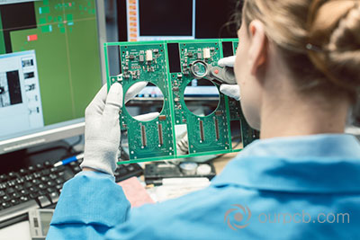
(Optical quality control and assembly inspection of an electronic product in the factory)
1. The Demand For AOI Testing
Over the years, we have improved the requirements of AOI and automatic optical inspection, so we cannot overemphasize it. The introduction of surface mount technology and further reductions in the size of these boards have made them compact, making it easy to miss obvious faults. Several solder joints in the PCB can find most of the errors.
In the past, we have conducted a manual inspection, but the increasing complexities of modern-day PCB tired-out inspectors made manual methods unreliable and, in the end, obsolete. Hence, there is a need to know automated test inspection through the seven aspects of knowing AOI testing procedures.
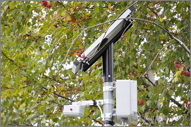
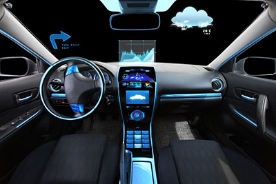
(motion detection system as one of the several applications of Printed Circuit Boards, PCB)
2. Working Principle of AOI Test
Automated Optical Inspection mimics the manual visual inspection you would otherwise do if you didn’t have this machine.
High-definition cameras inspect the PCB with light sources like LEDs, infrared, UV, or fluorescent illuminating the surface.
Once they capture a clear image, the computer compares it to the board’s parameters fed to it to identify errors or abnormalities.
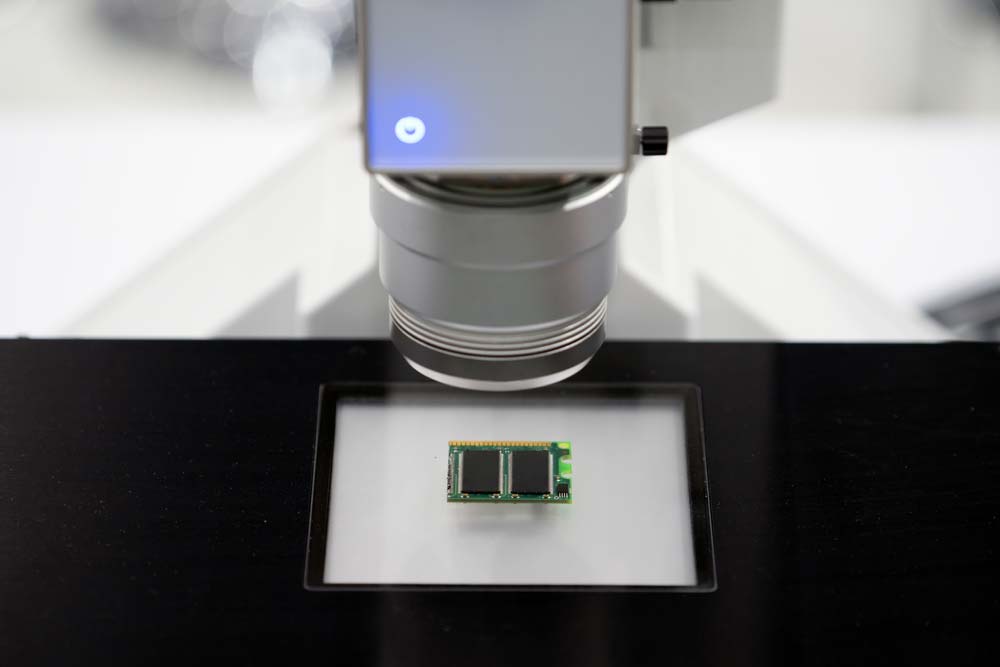
An Automated Optical Inspection system at work.
You can use different algorithms to do the comparison, but the most prevalent one is template matching.
This pixel-by-pixel method calculates the normalized cross-correlation between the two to determine if they match.
Object recognition and blob analysis follow a similar principle, but the latter separates the object from the background before comparison.
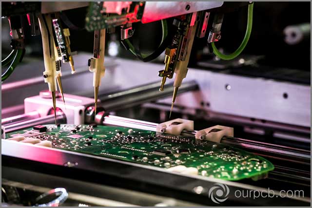
An automated vision system for PCB inspection after assembly.
3. Why Are AOI Tests Popular
Printed circuit boards are an integral part of automated optical test inspection.
When ordering the board, it should immediately correct its mistake. The financial implications of such things would be disheartening.
As mentioned earlier, due to the increasing complexity of modern circuit boards, manual inspection has become obsolete.
TNow points to check the circuit board by soldering automation. Contemporary markets now require high volume, top-notch products that can reach their customers as fast as possible without compromising quality inspection.
An automated test inspection is a fundamental tool in an electronics test strategy to ensure that faults are detected as fast as possible in production for products to reach the market in the shortest time possible.
(Printed Circuit Board with many electrical components)
4. The Advantages of AOI Test
AOI has become vital in PCB production because it has the following benefits.
Flexible Testing Method
AOI's primary application is checking the board after assembly, where you can analyze if there are anomalies or errors, such as missing components.
However, you can also use the process to inspect the PCB for copper trace anomalies after manufacturing.
High Positional Accuracy
Positional accuracy is critical in optical inspection systems because boards and their components are increasingly becoming tinier.
AOI cameras are powerful enough to detect minuscule deviations between the captured image and the template to check even the most advanced boards.
Programmable Lighting
You can reprogram the lighting or even use different light sources to give the cameras the best view of the board’s surface.
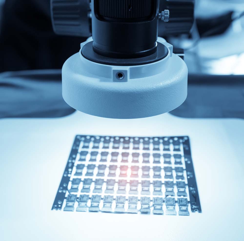
Machine vision and inspection using a high-resolution camera.
Reduces The Production Cost
Since this process is highly accurate, it helps you rectify tiny, unnoticeable issues that can be costly if they come out later during production.
5. Limitations of AOI Technology
Although AOI testing is highly accurate, it is not perfect. The cameras can miss some defects, especially if there is extremely low contrast between the images or at specific points.
But you can rectify this issue by adjusting the lighting or using different light sources to get the best contrast.
The computer algorithm can also confuse components and silkscreen markings on the surface, resulting in a false positive.
Lighting can cause shadows behind components because they protrude above the surface, which can be picked as anomalies.
The optical system only checks the surface, meaning it misses subsurface defects.
Similarly, its ability to inspect the liquid polymer underfill is limited. It can inaccurately report irregular PCB features that have no effect on performance.
6. AOI Test Application Areas
Automated Optical Inspection comes in handy when testing or checking the board for short circuits, line spacing violations, missing solder pads, line width violations, effects of high power loads and frequencies, and excess copper on the pads or lines.
These inspections usually come after manufacturing and component assembly.
7. AOI Test Detectable Defects
A wide range of errors can be detected using automated inspection test facilities. This involves using different techniques to determine if a printed circuit board fulfills all the conditions of quality or not. Some of these techniques include template matching, pattern matching, and statistical matching.
The template matching compares scanned images with the golden board. Pattern matching compares the information stored on both perfect and faulty systems. The statistical matching uses statistical data to address apparent problems.
Further advanced visual means for scanning a circuit board manufacturing defects.
The systems used for fault detection, on the other hand, also make use of images, comparing them with ideal diagrams in a bid to note some glaring faults.
- Welding defects can be detected in this way, for example, solder bridges, solder short circuits, the solder gap, excess solder, the solder mass, and an open circuit condition. To address these issues, the solderability test offers valuable insights into improving solder joint quality.
- Component defects are also addressed, such as missing components, incorrect component value, improperly placed or misaligned components, faulty parts, lifted lead deficiencies sent when aiming to correct errors in printed circuit boards.
- Also, BGA shorts and BGA open circuit connections can be detected during the AOI tests in line with approved guidelines and industry requirements such as understanding IPC standards, which define the quality benchmarks for PCB manufacturing and assembly.
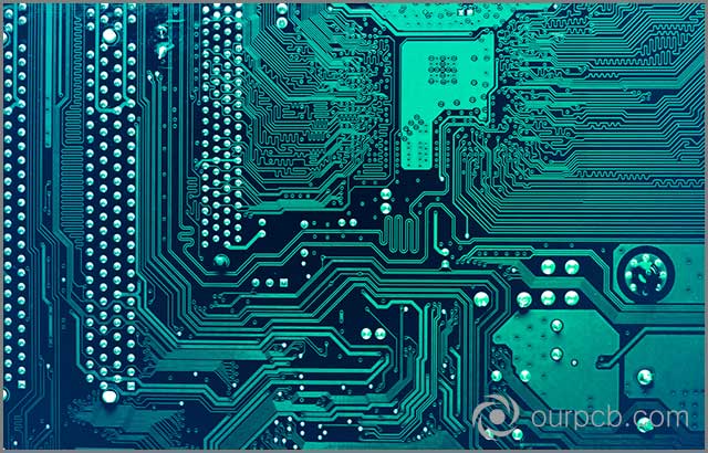
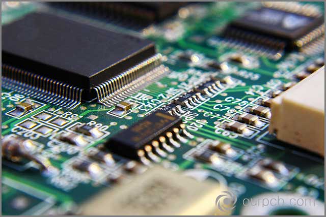
(printed circuit board, digital motherboard chip, and integrated communication processor)
Special Offer: Get $100 off your order!
Email [email protected] to get started!
8. The Technology Used When Checking or Testing
There are different technologies or means used for checking or testing for abnormalities in printed circuit boards. Some of these include In-Circuit Testing, which is a robust testing method.
Designed for full coverage testing PCB design, and the user is guaranteed about 85-90% coverage that is free from human error compared to other methods.
This test actuates the entire board circuitry, and it also involves the use of probes laid out expertly in a manner that mimics the design of the circuit board.
Experts have recommended that this test is ideal for a product that only needs a few revisions.
Other testing methods include:
- The flying probe test: This is cost-effective when compared to in-circuit testing. It is a non-powered test that is ideal for checking for Shorts, Opens, Resistance, Inductance, Diode issues, and any related checks to be carried out.
- The Burn-in Testing: This is an intensive test for printed circuit boards.Its designers to detect a load failure
- The X-Ray inspection testing: This method is the best for detecting soldering defects that are not visible to the naked eyes.
- Functional testing: This is a test that requires the use of external pieces of equipment, and it ensures that the PCB will power-up to perform its functions.
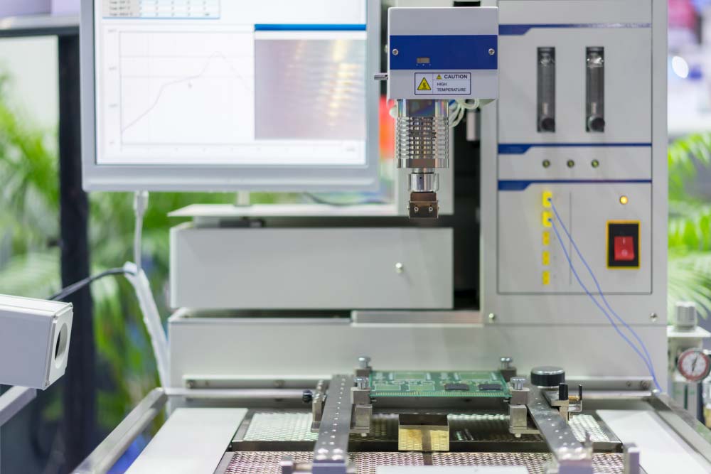
(flying probe test as a method of testing for defects in printed circuit boards)
9. Different Types of AOI Systems
Although the traditional 2D AOI systems are still effective at checking PCBs, 3D AOI is more precise because it is less affected by lighting and color variations.
2D AOI Systems
These systems rely on 2D cameras to capture PCB surface images for comparison and are effective at detecting things like missing or misaligned parts and soldering defects.
3D AOI Systems
These systems are expensive; that is their primary downside, but the precision of error detection is unmatched. You have the option of using laser triangulation or structured light projection.
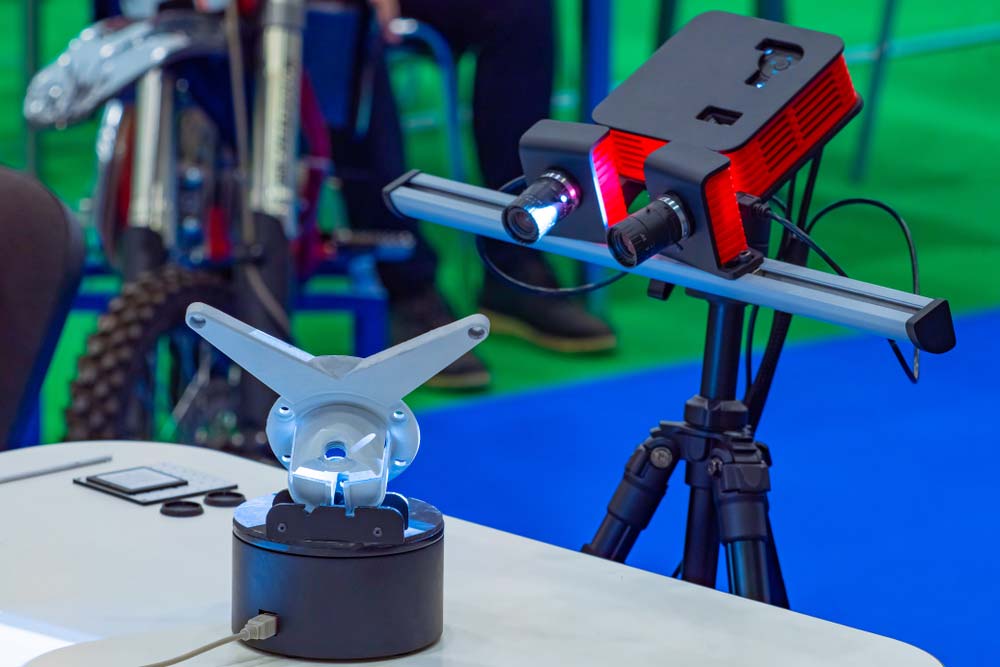
A 3D scanner acquires dimensional data from an object.
10. AOI Machine Types
AOI machines can be integrated into the production line to check the PCBs immediately after the surface-mount assembly process, which involves reflow soldering. These machines are known as inline AOIs.
Or you can use a standalone AOI, which is not hooked to the production line. This system samples a few boards from the assembly line to verify and certify the process.
You should consider the dual-lane AOI if you have a large production line that churns out multiple boards per day. You can also use this double-throughput system for redundancy; if one lane fails, you can still continue producing.
But for small production houses or even DIY PCB production, get the mini AOI benchtop system.
11. The Type of Lighting Systems Used for AOI Test
Light is one fundamental part of the automatic optical inspection layout.
Choosing the most appropriate amidst the available lighting systems is very crucial for easy detection of faults. Recently in lighting technology, we have made some progress.
To enhance the image-derived, reduce the time required to develop overall system status, and increase accuracy.
Many AOI systems in use have a well-defined lighting apparatus. Although this solely depends on the type of product to be tested and the operation carried out. Sometimes, when carrying out PCB quality testing, you may need to do some customizations, and the proper understanding of lighting would be required. The types of lighting used include:
- LED Lighting: An LED lighting system's use means that AOI systems can suitably adopt a stable form of lightning in carrying out random checks. By using LED lighting, we can easily control the light intensity. LEDs are better alternatives to fluorescent and incandescent lights. For applications like LED PCB, where precision and consistent lighting are crucial, LEDs offer a reliable solution. Although from experience, We noticed that the power of LED lights decreased over time. Nevertheless, we can add circuits to solve the problem.
- Fluorescent Lighting: This is one of the most widely used light sources for AOIs; adequate lighting means checking defects on PCB. However, the main drawback of this form of lighting is that it degrades over time. It means that the optical detection system may change over time.
- Ultra-violet or Infra-red light: This is useful to enhance certain defects, and third lighting systems are readily detectable.
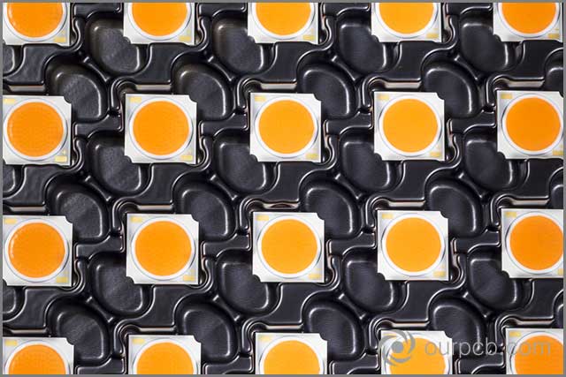
(Cob LEDs on black carrier trays as a type of lighting used for AOI)
12. AOI Camera Configuration
One of the fundamental and equally important aspects of the automatic optical inspection system is the image capturing system.
It enables capturing the image of the printed circuit boards and its assembly layout that is subsequently analyzed by the related software within the AOI system.
There are different types of AOI camera configurations used for image capture and analysis of the overall AOI system to detect faults in a PCB.
Based on examples using this setting, the imaging system may comprise a single camera. There is also the possibility of using multiple cameras to increase the chances of detecting an inherent fault.
A 3D camera provides better imaging. Any camera type used should be able to move under the control of application software to detect the faults. Speed and accuracy are also factors that influence the choice of cameras to use.
Camera types include:
- The still image-camera system: We need to place it near the target PCB, and its effectiveness depends on the existence of the sound lighting system. The camera might need to be under the control of an audio software system to ensure efficacy.
- Streaming Video: This is also another type of camera used for optical inspection. From the streaming video, full-frame shots are taken and subsequently analyzed. Conclusion this approach is not definite as it is not so accurate compared with other alternatives, but it possesses an advantage of speed over others.
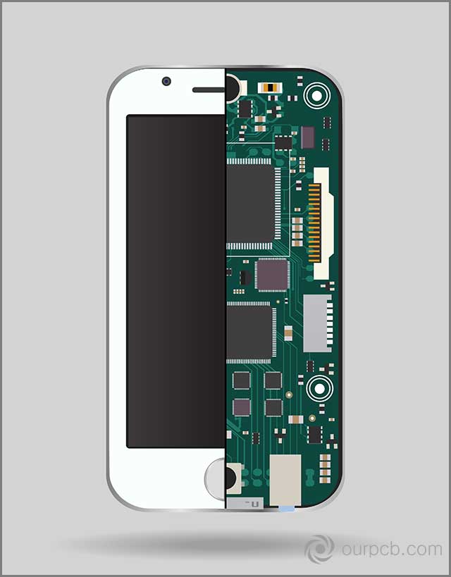
(Circuit boards configured into a mobile device)
13. AOI Test is Required Whether Prototyped or Soldering Process
Regardless of whether the assembly process follows the prototype, the AOI test is required.
Or it is a soldering process. No matter the intricacies involved, the optical inspection system is an automatic quality inspection that is best for checking out for inherent errors of manufacturing or other quality issues.
Product quality is the aim in this context, and automated optical inspection systems can ably provide that.
14. AOI Compared To Other Inspection Methods
Compared to X-ray inspection, AOI is cheaper and takes a shorter time to complete, as well; X-ray unearths subsurface defects that AOI cannot.
Put head-to-head with ICT (In-Circuit Testing), AOI finds superficial errors, and ICT detects electrical issues between the components.
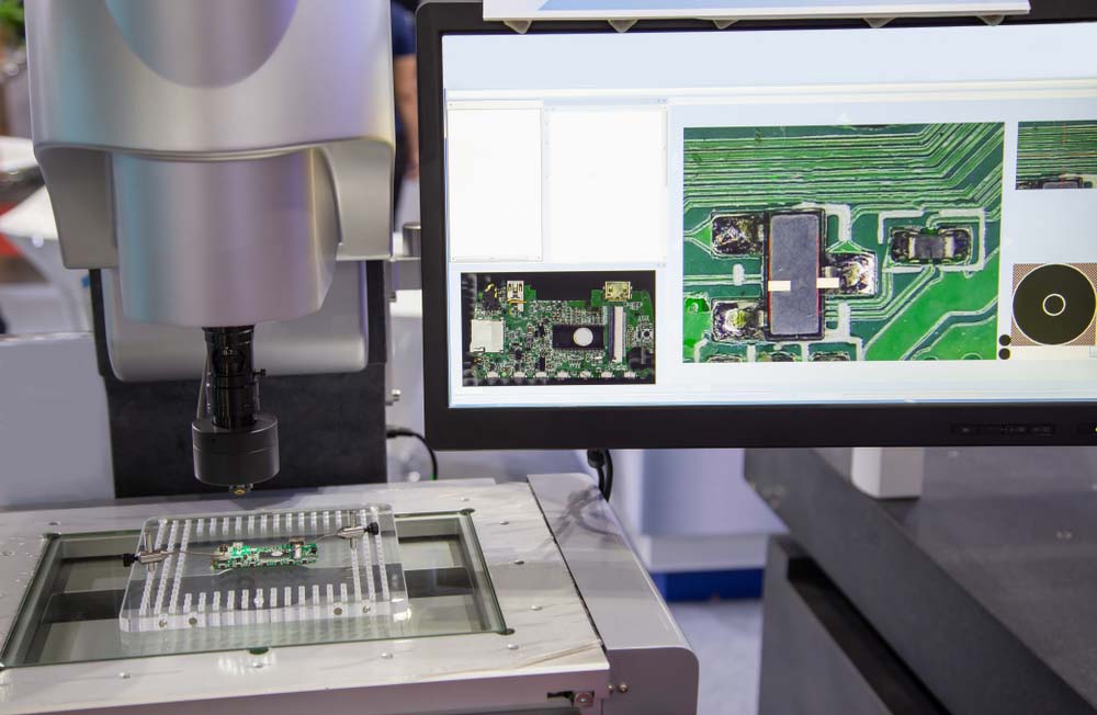
A visual measuring system using a high-res camera and bright lighting
Solder Paste Inspection is also critical in the production process, but it comes before component mounting to check the solder paste deposit quality; AOI comes after soldering.
15. AOI Test Cost
The cost of a complete AOI solution costs $30,000 going up; dual-lane and 3D systems are significantly more expensive.
Keep in mind these systems are ideal for high-volume production where the boards have low component variability, So only spend this money if your DIY project requires it.
Summary:
In conclusion, When checking the quality of manufacturing the printed circuit board, it takes a long time to fully accept the automated optical inspection system. The complexities of PCB have grown over time, improving the capacity for optimum functioning of AOIs.
The presence of smaller components and higher densities on contemporary PCB has further prompted the increasing acceptance of automatic checking systems. These facts have been discussed in this article to foster an increased understanding of its role. OurPCB has advanced detection technology; if you need it, you can contact us in time to get service.
Back to top: 15 Aspects To Help You Learn More About AOI Test
Special Offer: Get $100 off your order!
Email [email protected] to get started!