Contents
- What is the PCB Manufacturing Process?
- How does the PCB Design Process Influence Manufacturing?
- Key Elements in the PCB Design Process:
- What are Involved in PCB Fabrication and Assembly?
- The Lamination Process in PCB Fabrication
- Role of Copper Foil in the Fabrication Process
- Drilling and Plating
- Surface Finish Application
- Finalizing the Printed Circuit Board Manufacturing
- Multilayer PCB Manufacturing Process
- Challenges of Multilayer PCB Design and Manufacture
- What is the Importance of PCB Testing in the Manufacturing Process?
- How Testing Affects the Manufacturing Process
- How Manufacturing Affects PCB Testing
What is the PCB Manufacturing Process?
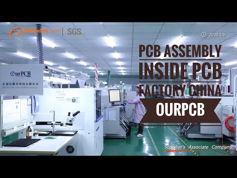
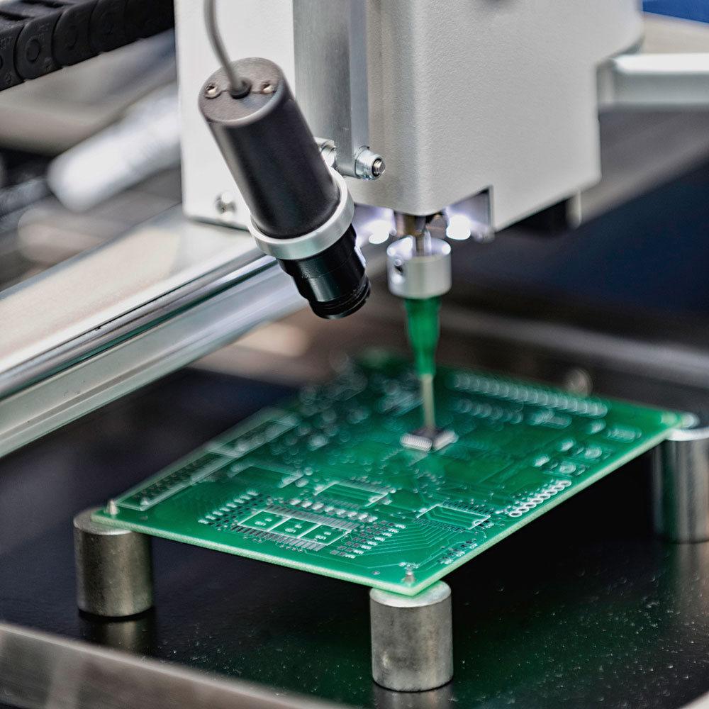
The PCB manufacturing process begins with the design phase, followed by manufacturing, assembly, and testing. Each phase utilizes specialized techniques to ensure that the production of PCBs meets industry standards and project requirements. Industrial-scale PCB production involves a complex series of specialized machines, materials, and processes to fabricate multilayer boards. Careful control and optimization of each step are crucial for achieving the desired electrical and mechanical performance of the final product.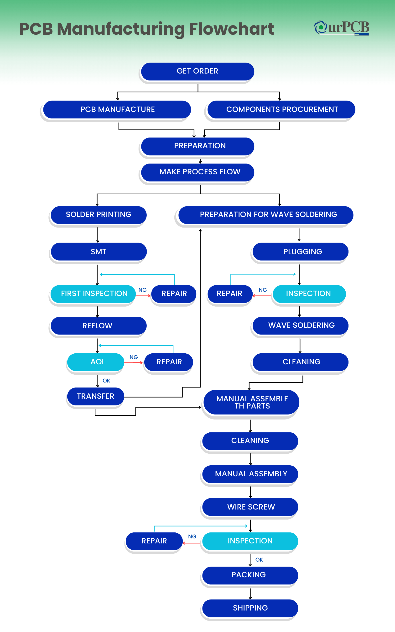
- Design and File Preparation: PCB manufacturing starts with the design. Engineers use software like CAD (Computer-Aided Design) to create the layout, defining where components go and how connections are made. The design is saved in a format, usually Gerber, that manufacturers use.
- Material Selection: The base material for the PCB is chosen based on the project’s needs. Common materials include FR4, CEM-3, and Rogers. The chosen material affects the board's durability and performance.
- Printing the Inner Layers: The design is printed on a photosensitive film that covers a copper-laminated board. UV light exposes the circuit pattern, and the film is developed to leave the copper traces behind.
- Etching: Excess copper is removed, leaving only the copper traces that form the circuit. This step ensures that only the desired paths for electrical connections remain.
- Layer Alignment and Lamination: For multi-layer boards, individual layers are aligned and laminated together. The layers are pressed and heated to fuse them into a single piece.
- Drilling: Holes for components or electrical connections are drilled into the board. The drilling process ensures that all holes are precise and correctly placed.
- Plating and Copper Deposition: A thin layer of copper is deposited inside the drilled holes and on the board’s surface. This connects different layers of the board and prepares it for component placement.
- Solder Mask Application: A solder mask is applied to protect the copper traces and prevent unwanted soldering. This mask is usually green but can come in other colors like black, blue, or red.
- Silkscreen Printing: Text, labels, and symbols are printed on the board to guide the assembly of components. This helps during the assembly and future repairs.
- Surface Finishing: A surface finish is applied to the PCB pads. Common finishes include HASL, Immersion Gold, and OSP. The finish improves the soldering process and protects the board from damage.
- Electrical Testing: The PCB is tested to ensure it works as designed. The tests check for open circuits, shorts, and proper connections.
- Final Inspection and Quality Control: The PCB is inspected for physical defects, such as scratches or misalignment. Quality control ensures the board meets the required standards before moving to assembly.
- Assembly and Packaging: The board is assembled with components like resistors and capacitors, either through Surface-Mount Technology (SMT) or Through-Hole Technology (THT). After assembly, the PCB is inspected again, packed, and shipped.
Special Offer: Get $100 off your order!
Email [email protected] to get started!
How does the PCB Design Process Influence Manufacturing?
The design phase greatly influences the PCB manufacturing process, determining the board's functionality, ease of production, and overall cost. A well-executed PCB design leads to smoother manufacturing, while poor designs may cause costly errors or delays.
Key Elements in the PCB Design Process:
- Schematic Design: This phase involves defining the electrical functionality of the circuit by creating a blueprint of how components will interact. The schematic ensures that the desired connections between components are logically sound and optimized for performance, serving as the foundation for the physical layout.
- PCB Layout: The PCB layout is the process of determining the physical placement of components and routing the electrical connections on the board. A well-planned layout ensures efficient use of space, optimal signal integrity, and heat management, all of which are crucial for manufacturability. The layout directly influences factors like cost, reliability, and ease of production during the PCB manufacturing process.
- Design for Manufacturability (DFM): DFM ensures that the design is optimized for production, minimizing potential complications during the PCB manufacturing and assembly stages. This involves taking into account factors like spacing, component placement, and material selection to ensure that the design can be easily and cost-effectively manufactured without sacrificing performance or quality.
A well-thought-out design streamlines PCB manufacturing process, ensuring efficiency and cost-effectiveness while avoiding complications like tight tolerances that can complicate the PCB production process and raise production costs and lower yield.
What are Involved in PCB Fabrication and Assembly?
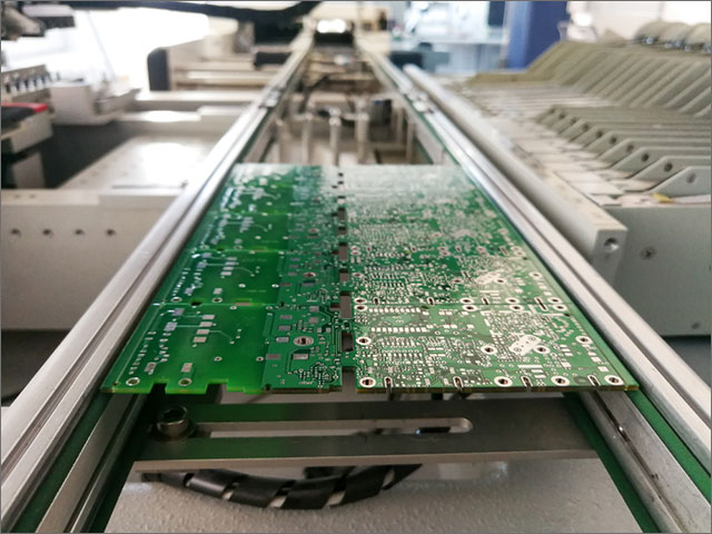
The manufacture of PCBs involves a sequence of precision-based tasks that must be executed correctly to ensure quality. Each step, from material selection to final testing, plays a crucial role in delivering a functional and reliable circuit board.
The Lamination Process in PCB Fabrication
Lamination is critical in multilayer PCB manufacturing, where multiple layers of copper and insulating material are bonded together under high pressure and temperature. This step ensures the mechanical strength and electrical integrity of the board by tightly bonding the layers, preventing delamination and signal interference between circuits. Proper alignment during lamination is essential to avoid defects such as misregistration of layers.
Role of Copper Foil in the Fabrication Process
Copper foil is a key material in PCB fabrication, as it creates the electrical pathways that connect the components. It is applied to the surface of the board, and specific areas are etched away to form the desired circuit patterns. Managing the thickness of the copper is crucial, as it affects the board’s current-carrying capacity and thermal performance, ensuring the board can handle the necessary electrical loads.
Drilling and Plating
Drilling is used to create holes, known as vias, that allow electrical connections between layers in multilayer PCBs. These holes are then plated with copper to create conductive pathways. This stage requires extreme precision, as improper drilling or plating can lead to connection failures or short circuits, impacting the board's overall functionality.
Surface Finish Application
A surface finish is applied to the PCB to protect exposed copper circuits from oxidation and to improve solderability during assembly. Common finishes include ENIG (Electroless Nickel Immersion Gold) and HASL (Hot Air Solder Leveling), which ensure long-term reliability and good electrical performance by providing a stable, protective coating.
Finalizing the Printed Circuit Board Manufacturing
After all the layers are laminated and etched, the final steps include applying a solder mask to protect the circuitry from environmental damage and prevent short circuits during soldering. A silkscreen layer is added to provide component labeling, assisting in assembly and troubleshooting. The completed board then undergoes final inspection and testing to ensure it meets the necessary electrical and mechanical specifications before it is assembled into the final product.
Multilayer PCB Manufacturing Process
A multilayer PCB consists of multiple layers of circuitry, allowing for more complex designs in a compact form. These boards are essential for advanced electronics, enabling high functionality while maintaining a small footprint.
The manufacturing process for multilayer PCBs are the following:
- Layer Stacking: Alternating layers of conductive copper and insulating materials (usually prepreg) are carefully stacked in the desired configuration.
- Lamination: The stacked layers are bonded together through a high-pressure and high-temperature lamination process, forming a solid multilayer structure.
- Drilling: Holes, known as vias, are drilled through the layers to create electrical connections between different layers of the PCB.
- Plating: The drilled vias are plated with copper to ensure proper electrical conductivity between layers.
- Etching: Excess copper is etched away from the surface, leaving behind the desired circuit pattern on the outer layers.
- Solder Mask Application: A protective solder mask is applied to insulate the copper traces and prevent accidental short circuits during component assembly.
- Surface Finishing: A surface finish, such as ENIG (Electroless Nickel Immersion Gold) or HASL (Hot Air Solder Leveling), is applied to protect the exposed copper and enhance solderability.
- Final Inspection: The completed PCB undergoes rigorous inspection and testing to ensure that it meets the necessary electrical and mechanical specifications before moving on to assembly.
Making a single-layer PCB is much easier than a multilayer PCB because it only has one layer of circuits, so there's no need to stack layers or drill holes to connect them. The process is faster and cheaper, involving just basic steps like etching and finishing. Multilayer PCBs, on the other hand, need careful alignment of layers and extra steps to connect them, which makes the process more complicated and expensive.
Challenges of Multilayer PCB Design and Manufacture
Manufacturing a multilayer PCB presents several challenges different from simple single layer PCBs.
- Precise Layer Alignment: Ensuring exact alignment during the lamination process is critical, as any misregistration of layers can lead to circuit failure or short circuits.
- Thermal Management: Managing heat buildup is more difficult in multilayer PCBs due to the increased number of layers, requiring careful design to ensure proper heat dissipation and avoid overheating.
- Electrical Performance Balance: Balancing the electrical performance of each layer while maintaining manufacturability is challenging, as different layers may have varying functions like power distribution or signal routing, which must all work together without compromising reliability.
- Complex Fabrication Process: The increased number of layers adds complexity to the fabrication process, including more intricate drilling, plating, and inspection steps to ensure quality and functionality across all layers.
What is the Importance of PCB Testing in the Manufacturing Process?
PCB testing is crucial for ensuring each board works as expected and meets quality standards. It helps catch defects like shorts, open circuits, or misplaced components that could cause the board to fail. Without proper testing, faulty boards could reach customers, leading to costly recalls or product failures.
How Testing Affects the Manufacturing Process
PCB testing can extend the manufacturing process because each board must undergo thorough checks. These additional steps add time but are essential for preventing defects, reducing the risk of producing faulty PCBs that could fail during operation. However, testing ultimately saves time by minimizing the number of returns, repairs, and rework, ensuring that boards leaving the production line are reliable.
How Manufacturing Affects PCB Testing
Conversely, the complexity of the PCB manufacturing process can also affect the testing phase. Multilayer PCBs or more detailed designs require stricter testing to ensure all layers and components function properly. Manufacturing variations in tolerances or materials can make defects harder to find, making extensive testing even more important to catch potential issues before the boards are shipped.
In summary, while testing can slightly extend the production timeline, it is a necessary step that greatly enhances the reliability of the final product. It also acts as a feedback loop, allowing the PCB manufacturer to adjust processes based on recurring issues detected during testing.
Back to top: PCB Manufacturing Process
Special Offer: Get $100 off your order!
Email [email protected] to get started!


