About Ultra-Thin PCB, Portable devices like smartwatches, tablets, laptops, and smartphones need thin circuit boards to form small, lightweight designs.
So, the conventional PCB thickness won’t cut it. This requirement led to the development of ultra-thin printed circuit board assemblies, which are up to the task.
Let’s look at the PCBs benefits, PCBs types, PCBs manufacturing/PCBs assembly considerations, and PCBs quality standards.
Contents
- What Is an Ultra-Thin PCB?
- Types of Ultra-Thin PCBs
- Ultra-Thin Rigid PCB
- Ultra-Thin Flexible PCB
- Ultra-Thin Rigid-Flex PCB
- What Is the Difference Between Single-Sided Ultra-Thin PCB and Double-Sided Ultra-Thin PCB?
- What Is the Thinnest PCB Possible?
- Advantages of Ultra-Thin PCBs
- Disadvantages of Ultra-Thin PCBs
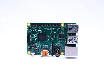
- Ultra-Thin PCB Common Applications
- Factors To Consider When Manufacturing and Assembling Ultra-Thin PCBs
- Substrate Material
- Copper Layer
- Vias
- Component Placement
- Trace Width/Spacing
- Solder Mask
- Thermal Management
- Flexibility
- Manufacturing Process
- Testing
- Dielectric Materials Used for Ultra-Thin PCB
- How To Drill Microvias Into Ultra-Thin PCB
- Plasma Etching
- Photo-Via Drilling
- Laser Drilling
- What Is the Purpose of Shielding in Ultra-Thin PCBs
- What Is Impedance Control in Ultra-Thin Printed Circuit Boards
- Ultra-Thin PCB Quality Standards
- IPC-6013
- IPC-6012
- IPC-A-600
- ISO 9001
- RoHS
- UL Guidelines
- REACH
- Wrap Up
What Is an Ultra-Thin PCB?
As the name suggests, extra or ultra-thin PCBs are circuit boards with a narrower thickness than regular boards.
Manufacturers achieve this narrow board thickness by reducing the width of the board’s base material, surface treatment, and conductive copper layer. Similarly, assemblers must keep up with this design by mounting low-profile components on the surface.
This PCB design is ideal for applications requiring miniaturization while maintaining high reliability.
Types of Ultra-Thin PCBs
Three types of PCBs adopt this ultra-thin design.
Ultra-Thin Rigid PCB
The thickness of this PCB makes it challenging to create a rigid structure. Therefore, manufacturers make them as packaging substrates for integrated circuits, which helps make the structure extremely thin.
You can make 25-micron broad areas, 50 microns on vias, below 175 microns for pitches, and 100 microns for pad diameters.
Ultra-Thin Flexible PCB
The ultra-thin PCB substrate material for this type must have flexible properties, and the typical ones include:
- Thin conductive copper layers
- Polyimide
- Adhesive
These board materials form a foldable structure that minimizes the installation surface area.
Ultra-Thin Rigid-Flex PCB
These PCBs have some parts rigid and others flexible. They usually feature plated thru-holes stretching across the rigid and flexible sections, enabling electrical connections in the multi-layered structure.
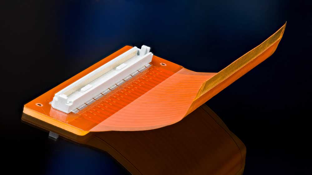
A rigid-flex PCB with the connector on the rigid section
The rigid sections provide hard surfaces for mounting the chassis and electronic components, while the flexible parts enable bend-to-fit applications or create vibration-resistant zones.
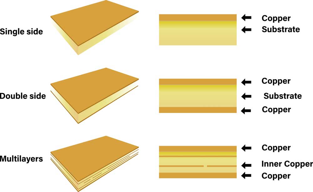
What Is the Difference Between Single-Sided Ultra-Thin PCB and Double-Sided Ultra-Thin PCB?
Single-sided ultra-thin PCBs have copper traces and electronic components fixed on one side of the board. But double-sided ultra-thin PCBs have two copper layers, one on either side of the substrate.
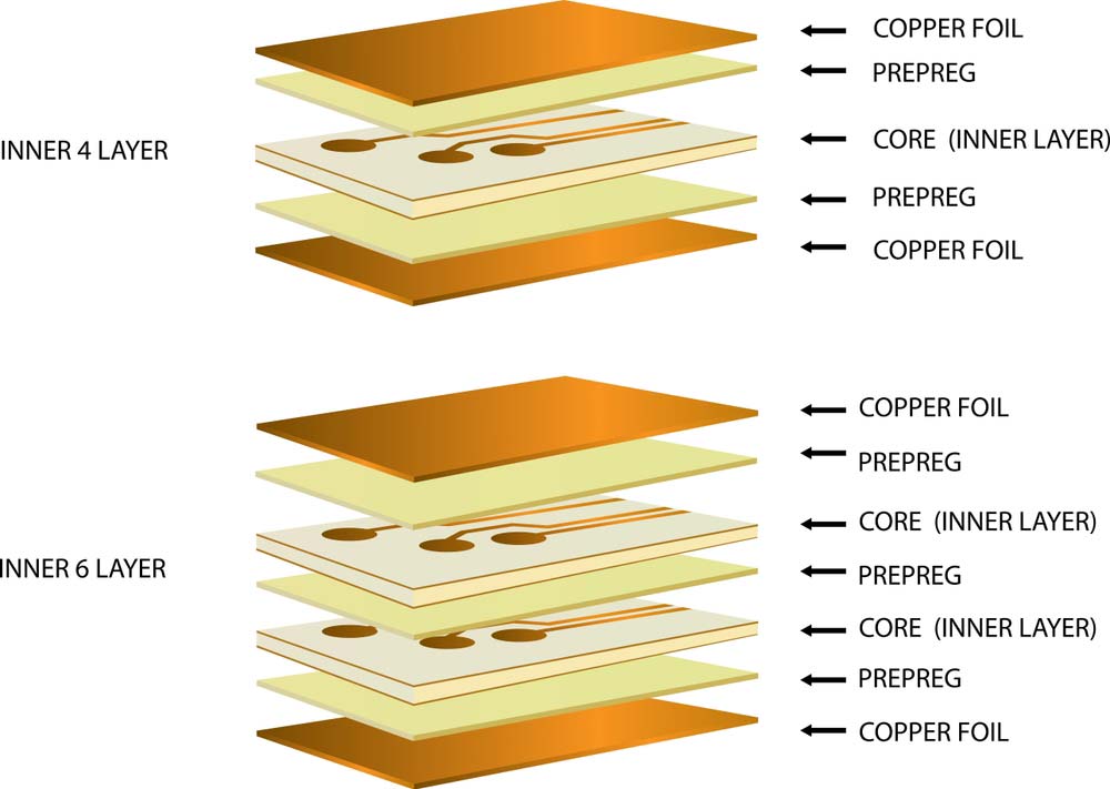
Circuit board layers in double-sided PCBs (note the two copper foil layers)
What Is the Thinnest PCB Possible?
The thinnest PCB possible is 0.2mm thick. Usually, the minimum circuit board thickness falls within the 0.3 to 0.4mm range, but ultra-thin PCBs are slightly thicker.
Regular PCBs have a thickness of about 1mm to 2mm, so ultra-thin boards fall under this range (below 1mm) and are slightly thicker than the thinnest possible board to be practical.
Three thin PCBs
Advantages of Ultra-Thin PCBs
- Short assembly time: Ultra-thin circuit boards feature configured lines that save time when linking excess lines.
- Lightweight design: Thin boards have tiny vias and small via-hole aspect ratios, narrow copper layers, and small lines/spaces, resulting in a light structure.
- Compact structure: Eventually, the lightweight design minimizes the board’s volume, making it compact and easily portable
- Efficient heat dissipation: Heat flows out quickly through the thin layers.
- Low cost: Reduced material usage cuts costs.
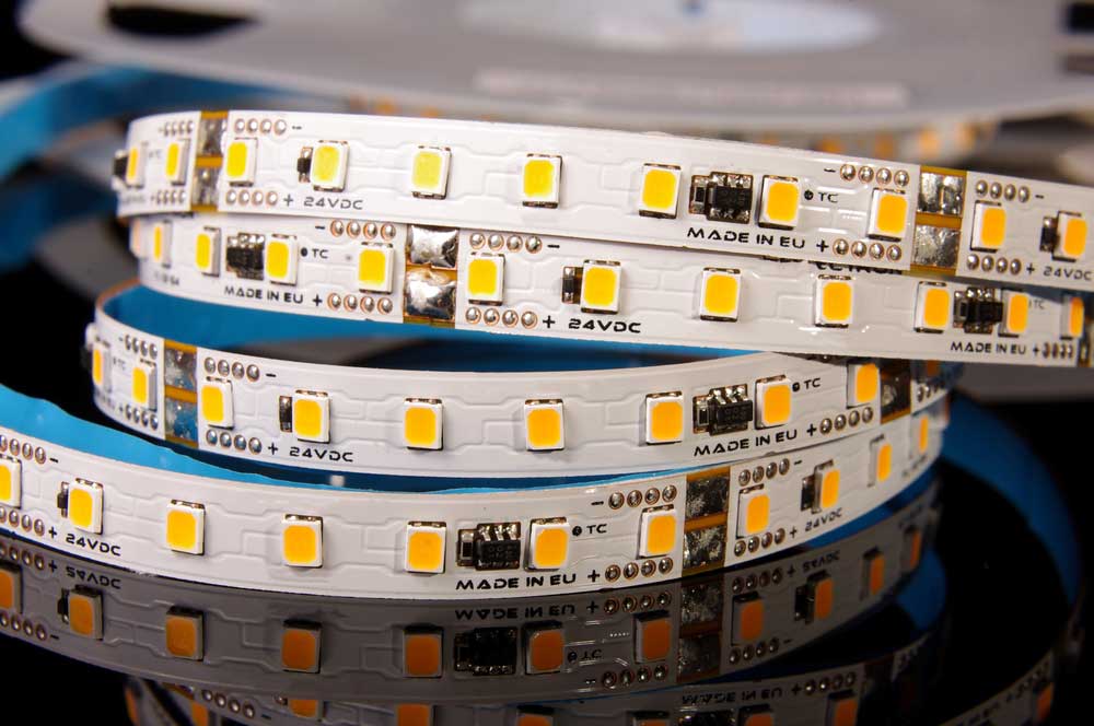
LEDs mounted on a thin, flexible, ultra-thin circuit board
Other benefits include good solderability and easy component assembly
Disadvantages of Ultra-Thin PCBs
This design is not without its drawbacks, which include:
- Signal losses
- Complex manufacturing
- Fragility
- Difficult to do repairs
- Design limitations
- Challenging temperature/thermal management
- Limited size
Special Offer: Get $100 off your order!
Email sales@ourpcb.net to get started!
Ultra-Thin PCB Common Applications
These boards have the following applications.
- Metro coins
- TF cards
- SIM cards
- NFC technology
- GPS devices
- Wearables
- IoT devices
- Mobile phone chargers
- Barcode equipment
- Medical devices
- Sensor cards
- Contact smart cards
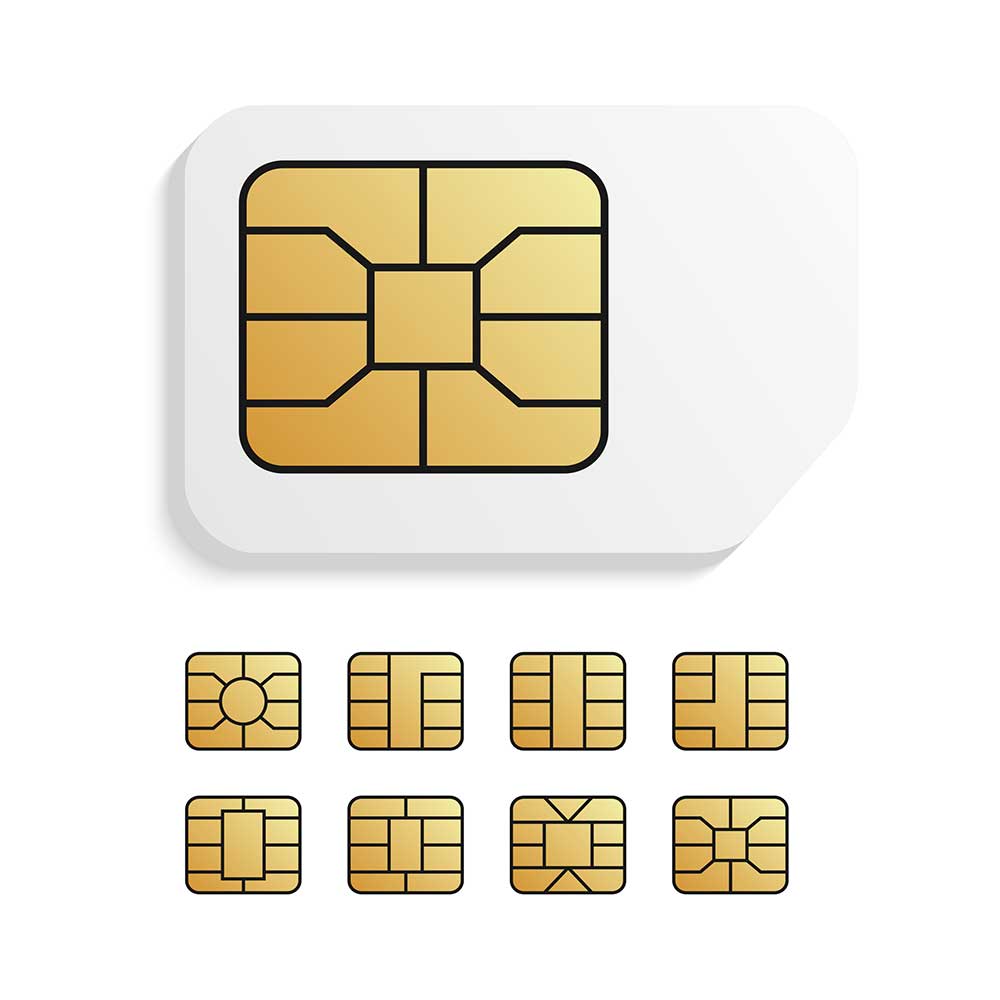
A phone SIM card
Factors To Consider When Manufacturing and Assembling Ultra-Thin PCBs
These factors are critical when manufacturing and assembling these ultra-thin circuit boards.
Substrate Material
The substrate PCB material is the board’s core that holds the components and copper traces.
Although you should use thinner substrate materials than the ones in regular circuit boards, they should be stiff enough to prevent flexing.
However, bending should not be an issue if making a flexible board.
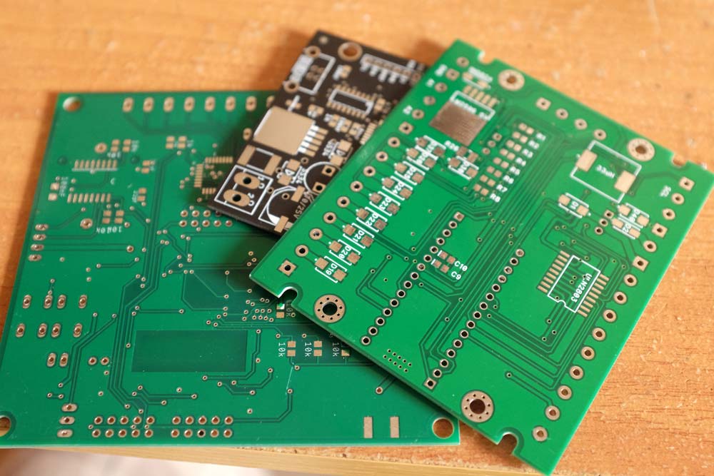
PCB materials in single, double, and multi-layer circuit boards
PET (polyethylene terephthalate), polyimide, and FR4 core materials are typical for this board construction.
Copper Layer
The boards also have thinner copper foils than the ones in regular PCBs.
Depending on the board applications, this layer’s thickness should range between 9 and 18 microns.
Vias
Drilling vias is challenging in ultra-thin boards because it can weaken the substrate and copper layers.
But you can’t do without them because they enable signal and power transmission between the copper layers.
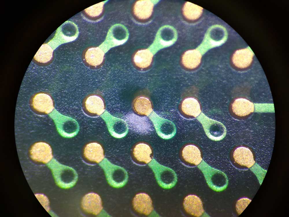
PCB pads and vias under a microscope
Therefore, you should carefully place and size the vias. Also, the hole’s diameter must be as tiny as possible, and the via should be as close as possible to the electronic components.
Component Placement
Component placement is critical because it determines the overall thickness of the board.
So, you should only use surface-mount components that have a thin profile. And install them near the PCB surface.
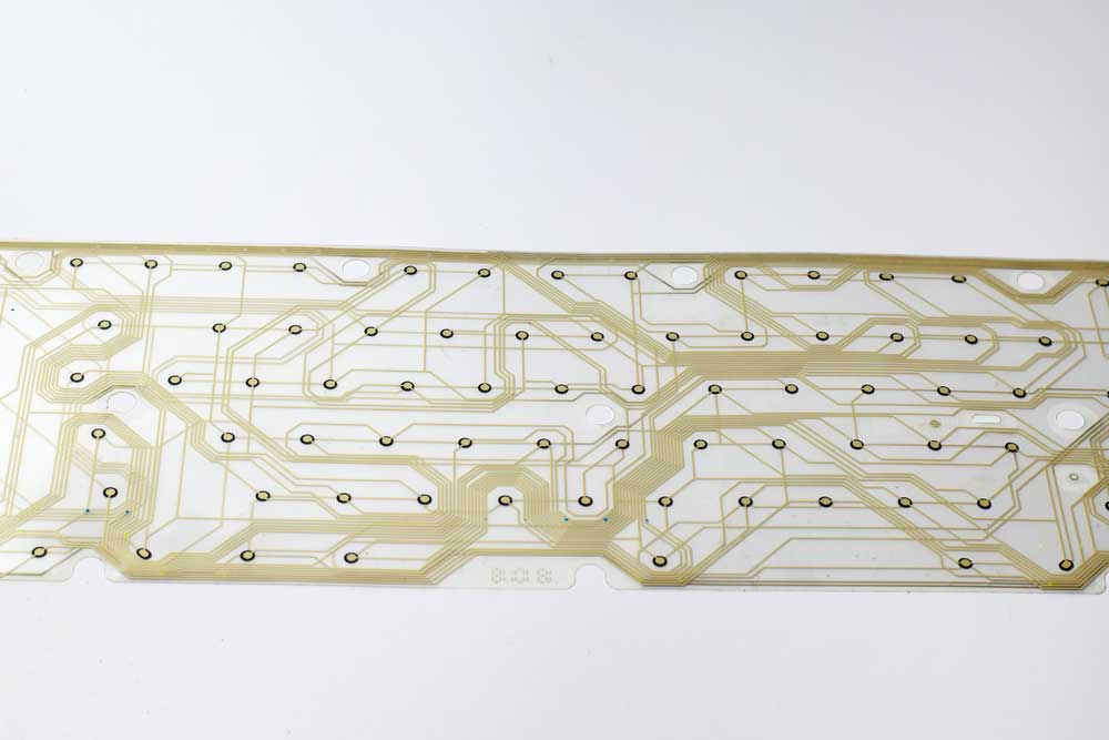
Trace Width/Spacing
Calculate and evaluate the width of the transmission lines accurately to ensure you install an etched copper foil thickness that can handle the required electrical current without overheating.
A flexible PCB (note the conductor trace width and spacing)
While at it, calculate the optimal trace spacing to prevent cross-talk or electromagnetic interference in different circuits.
Solder Mask
This masking is critical in circuit boards because it protects copper pads and traces from oxidation.
Since we arediscussingt ultra-thin PCBs, this layer should be as thin as possible to keep the board within the required parameters.
Thermal Management
Electronic components don’t function optimally when under heat stress. They can even get damaged.
So, it is essential to implement thermal management mechanisms in PCBs to prevent this shortcoming, and the ultra-thin type is no different.
Although the thin nature of these boards simplifies heat dissipation, implementing the thermal management mechanisms is challenging.
Heat dissipation requires cooling structures like thermal vias and heat sinks, which are challenging to install on the thin board.
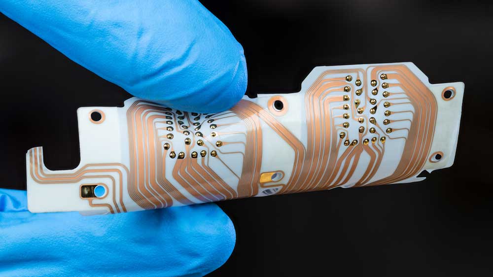
Flexibility
Flexibility might be essential in some applications, especially those with space limitations.
In such a case, manufacture rigid-flex or flexible circuits without compromising the board’s structural integrity.
A flexible keyboard PCB
You’ll have to use flexible materials and arrange the components carefully on the surface.
Manufacturing Process
Fabricating these boards is more complex and requires stringent measures than making regular-thickness PCBs.
Plus, you must have specialized manufacturing tools, thin copper foils, and thin substrate materials to fabricate the structure.
Some required tools include specialized via-hole drilling technologies that can handle photo-via, plasma, or laser drilling.
Testing
Ultra-thin circuit boards require careful handling because they have delicate structures. So, it would be best if youweree cautious when testing them to prevent manufacturer or assembler-related damages.
The most effective way to go about this testing process is to purchase specialized testing equipment to handle these custom circuit board.
Dielectric Materials Used for Ultra-Thin PCB
The common dielectric materials used to provide insulation and structural support in ultra-thin PCBs are polyester (PET), polyimide, and FR4. All three are epoxy-based and can either be reinforced or non-reinforced, a factor that affects the circuit board’s cost.
However, different applications require PCBs with different electrical, mechanical, thermal, and chemical properties. So, you can find boards with composite, aramid, or glass substrates.
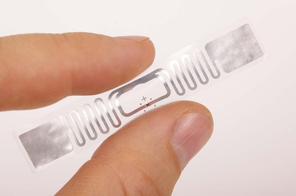
A thin, flexible RFID PCB
For instance, you might need some ultra-thin PCBs in a rigid state and others in a flexible design. Depending on the application area, you might need the board to resist certain chemicals or maintain maximum dimensional stability. All these factors will help you determine the most suitable dielectric to use.
How To Drill Microvias Into Ultra-Thin PCB
The thin nature of these boards requires specialized micro via drilling, and you can use either of these steps.
Plasma Etching
This method involves drilling the via-hole by etching the material using plasma in a vacuum, and it can create a 0.75µm (0.00075mm) hole diameter on 0.25µm (0.00025mm) thick materials.
However, the process has one major flaw: high cost. The cost of purchasing the vacuum machinery is quite high.
Photo-Via Drilling
Photo-via drilling involves using lithography patterning to create the holes on a photo-imaginable dielectric material.
The process is efficient and effective at boring tiny holes that measure 25µm in depth and diameter.
However, it has one downside: the photo-imaginable dielectric material is expensive, which means the ultra-thin PCB will be costly to the end user.
Laser Drilling
Laser drilling is the best and most preferred microvia drilling method on ultra-thin PCBs. It can create narrow holes with a 5µm diameter and a similar depth through the dielectric.
The process involves focusing a laser beam on a tiny dielectric section. It creates clean holes that form uniform and even conductive surfaces when metal-plated.
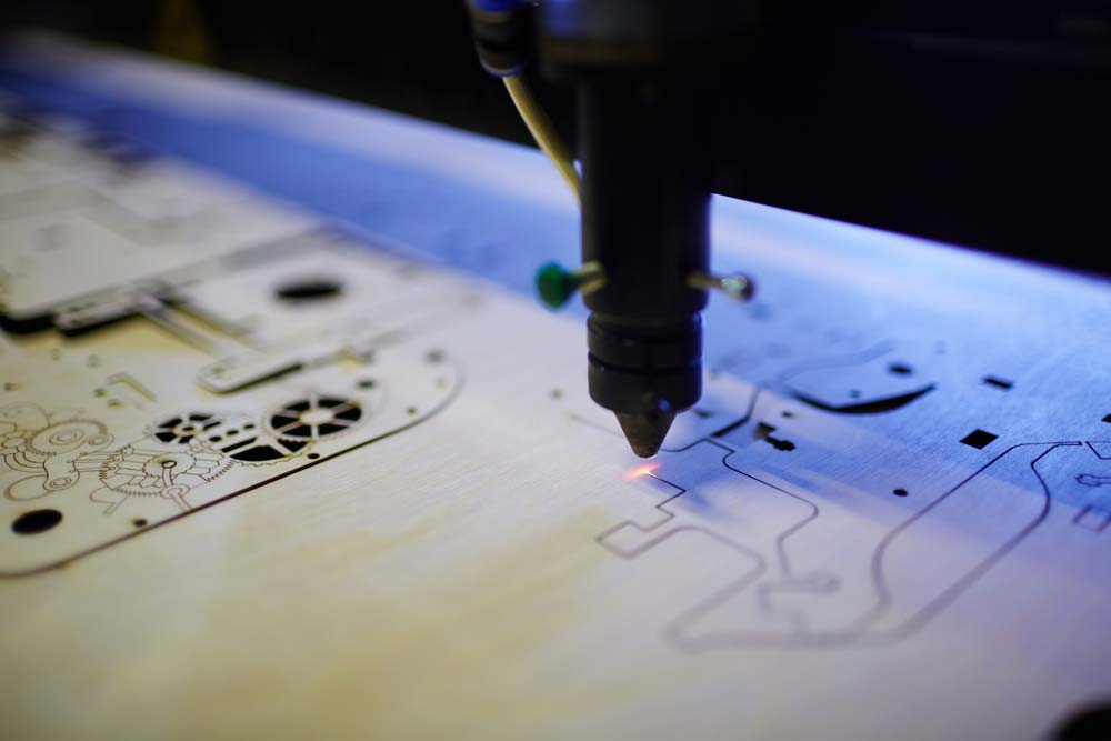
A laser cutter projecting a narrow beam on the working surface
You can control the laser microvia drilling process by adjusting the beam’s wavelength, which alters energy density. So, it is possible to drill denser microvias.
However, lasers have a limited depth, which makes it difficult to drill past a certain depth. The only solution is to use a collimated laser. However, the tiny hole’s diameter can cause Fresnel diffraction, impacting the beam density and its ability to cut deep.
What Is the Purpose of Shielding in Ultra-Thin PCBs
Since these boards are thin and have limited or no layers to protect against electromagnetic interference, external noise sources can significantly impact their performance. Therefore, shielding is important to maintain signal integrity.
Radiofrequency shielding enclosures
This shield is an electrically conductive layer between the EMI source and the PCB to reflect ab,sorb, and ground these noise signals.
What Is Impedance Control in Ultra-Thin Printed Circuit Boards
The process primarily involves checking and coordinating the locations and dimensions of the board’s traces to match the specific substrate that forms the base.
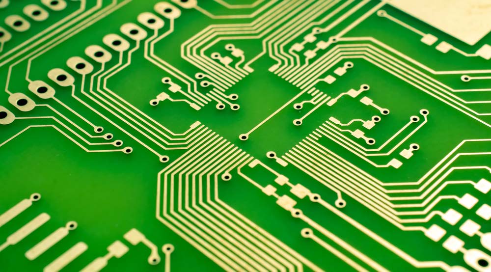
Copper traces on a PCB
Impedance control in ultra-thin PCBs ensures the signal transmitted along the copper traces does not surpass a specific range.
This control is critical when handling high-frequency signals, such as for Bluetooth or Wi-Fi transmission.
Ultra-Thin PCB Quality Standards
These circuit boards must adhere to the following quality standards to guarantee performance, quality, and reliability.
IPC-6013
This standard specifies the quality and performance of flexible and rigid-flex PCBs. Some flexible PCB specifications cover the ultra-thin type in the following areas.
- Design
- Manufacturing
- Performance
- Testing
- Components
IPC-6012
If you recall the ultra-thin PCB types, there is a rigid ultra-thin board. The IPC-6012 specification covers the design, manufacturing, performance, testing, and component performance of non-flexible boards, which include the ultra-thin subcategory.
IPC-A-600
This guideline defines the acceptance criteria for PCBs, creating a benchmark for manufacturers and buyers.
Specifically, this standard lists the visual criteria for examining and assessing PCB quality (including ultra-thin types), such as their craftsmanship.
ISO 9001
ISO 9001 lists the quality management standards for companies, including the ones that manufacture and assemble ultra-thin circuit boards.
Therefore, this standard ensures these boards have a constant level of quality.
A set of ISO-certified badge stamps
RoHS
RoHS is an acronym for Restriction of Hazardous Substances Directive, an EU directive that forbids several hazardous materials in manufacturing electrical and electronic equipment.
Ultra-thin PCBs fall squarely in this category, and adhering to these standards means the structure does not have harmful materials like Lead, cadmium, and mercury.
UL Guidelines
UL (Underwriters Laboratory) is a third-party certification company that rigorously tests products and machines to meet the required performance, sustainability, and safety standards.
Therefore, a UL-certified badge on an ultra-thin PCB gives you confidence in the product’s performance and reliability in the long run.
REACH
REACH adds to the effectiveness of RoHS to ensure ultra-thin PCBs are free from harmful chemicals.
The EU legislation is an acronym for Registration, Evaluation, Authorization, and Restriction of Chemicals.
It guarantees the safe incorporation of harmful chemicals into products like ultra-thin PCBs.
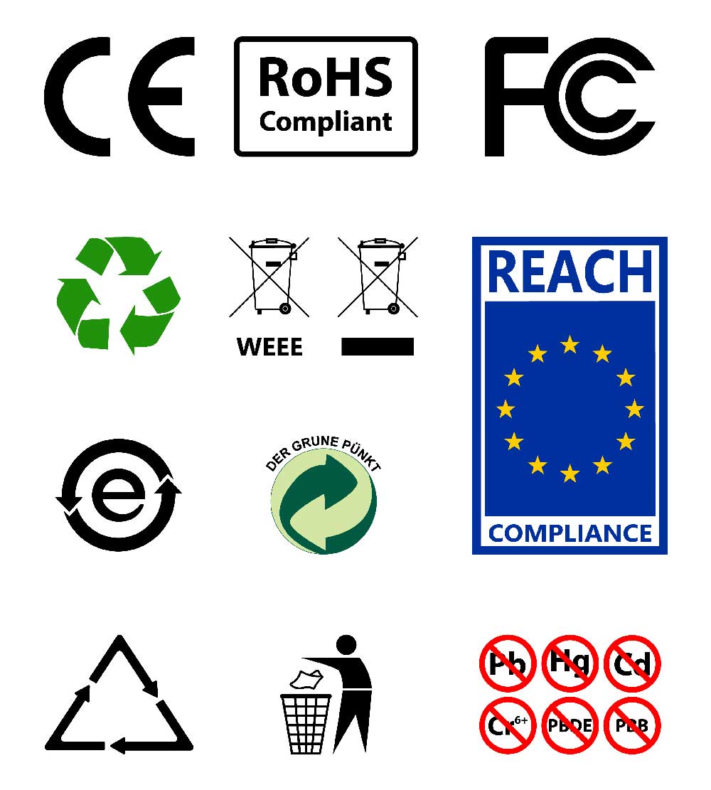
Multiple quality standard certification standard badges, including REACH and RoHS
Compliance means these circuit boards have zero toxic substances that can endanger your health.
Wrap Up
Ultra-thin PCBs are critical for compact, portable devices, but you must follow strict manufacturing and assembly guidelines to ensure proper functioning.
Making these boards have a rigid structure is more challenging because of the thin substrate material layer.
But, the flexible ones are easier to fabricate, although they have their fair share of issues. Please goo through this rigid-flex PCB manufacturing guide to learn about our fabrication abilities, or contact us for more information.
Special Offer: Get $100 off your order!
Email sales@ourpcb.net to get started!