Have you heard the term capacitance? Before we plunge into the discussion of capacitance and stray capacitance, it is essential to understand what a capacitor is.
A capacitor is a vital electronic part that takes full advantage of multiple electric fields' ability to reach across an insulator (Ng and Saran, 1996). Capacitors (often called condensers) are energy-storing components used widely in TVs, radios, and other electronic equipment.
We will discuss capacitance and stray capacitance in detail and their implications on PCB circuits.
Contents
1、What is Stray Capacitance?
Capacitance is the property of a set of conductors or an electric conductor measured accurately by the quantity of separated electric charge (Geaghan, 2013).
Capacitance is often stored on it per unit change or fluctuation in electrical potential.
It is worth mentioning that capacitance also indicates related storage of electrical energy.
Stray capacitance is a type of capacitance; unwanted, excess, or preferably unavoidable and is induced in various electronic components because of their parallel alignment, typically known as stray capacitance.
Stray capacitance is a special measurement error often defined as the capacitance between different connections in a fixture or/and the tip of the tweezers.
A reasonable amount of stray capacitance is added to the measurement of a capacitor if the institution is open.
Having said that, if the compensation opens fully implemented, it can be accurately compensated by the stray capacitance generated in the jig.
Engineers know that a high-frequency system that operates in RF and a microwave spectrum usually encounters this effect.
In inductors, stray capacitance generates a series of resistance, while in PCB, it is common to see that induced capacitance changes its operating point.
All main circuit elements like diodes, inductors, and transistors tend to have internal capacitance, which could cause their behavior or pattern to depart a little from 'ideal' circuit elements.
Also, there is a non-zero capacitance between the two conductors (McAllister, 1991).
Remember that this may be significant or more pronounced at a higher frequency, especially when conductors are closely spaced, such as printed circuit board or wires traces.
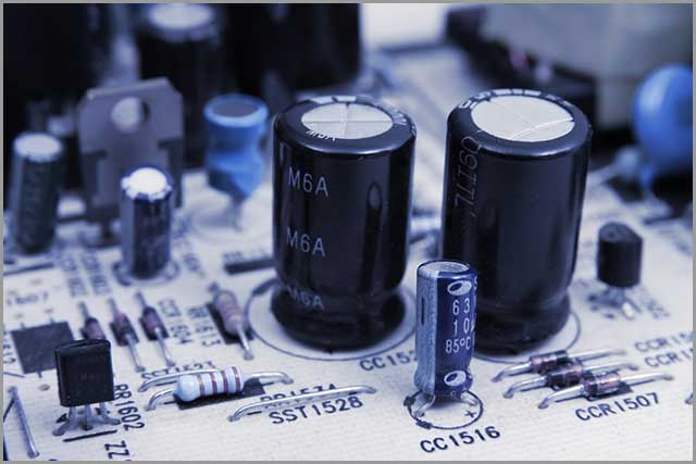 Image 1: Stray Capacitance
In PCB
In high-voltage and high-frequency systems, conductors do not need another conductor to produce capacitance between them. It is because it is induced merely by interaction with the environment.
Note that in Printed Circuit Boards (PCB), this often results in plenty of unwanted or unnecessary capacitance that may impact the performance of a system.
Electronic design automation computerized programs used in designing most commercial printed circuit boards could calculate the stray capacitance and other parasitic impacts of both circuit board traces and components and tend to include them invaluable simulations of circuit operation. This is parasitic extraction (Kao, Lo, Singh, & Basel, 2001).
It is worth noting that stray capacitance could usually be ignored; Having said that, in many high-frequency electric circuits, it might turn out to be a huge problem.
In most amplifier circuits with extended frequency responses, the stray capacitance between the input and the output may act as an active feedback path, which causes the electrical circuit to oscillate at a higher frequency frequently. Remember that these unwanted and unavoidable oscillations are known as parasitic oscillations (Palmer & Joyce, 2003).
Using the figure below, we can easily calculate the stray capacitance in any PCB substrate. Note that this capacitance may theoretically be used in a variety of places that need small discrete capacitors, but it is, in most cases, an inefficient way.
Also, high-frequency systems may generate capacitance between their bottom and top layers; Having said that, because of the insulation between these layers, it would be in the negligible range of about three pF per cm2.
Now we will discuss the effects.
Effects
It is important to remember that in most higher frequency amplifiers, the stray capacitance may combine easily with some stray inductance, like component leads, to form various resonant circuits, which can also lead to a parasitic phenomenon oscillations.
In almost all inductors, the parasitic capacitance may resonate with the inductance at some high frequency to make an inductor self-resonant, known as the self-resonant frequency. Above this specific frequency, the inductor has capacitive reactance.
Designers of electric circuits try their best to minimize or eliminate stray capacitances, if possible. They often do this by carefully keeping all of the leads of electronic parts concise and grouping these parts in a way that eliminates capacitive coupling. The stray capacitance of a load circuit attached firmly to the output in op-amps may lower their bandwidth.
Most high-frequency electric circuits need specialized design techniques like careful separation of components and wires, guard rings, power planes, ground planes, shielding between output and input, and termination of strip lines and lines to minimize the impacts of unwanted capacitance.
We have covered a lot of territory in this section. The next section will discuss the differences between stray and parasitic capacitance. Although these terms are often used interchangeably, there are some critical differences that you should know.
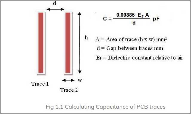 Image 2: Stray Capacitance
2、Difference Between Stray and Parasitic Capacitance
When two electrical conductors or parts are in physical proximity, carry a charge, and have a specific voltage potential between them, they will likely produce a virtual capacitor; this is true even if all the conductors are adequately insulated.
Note that the virtual capacitor between these conductors is often called parasitic capacitance.
Parasitic capacitance is unavoidable, excess, and unwanted capacity between 2 or more electrical conductors, which tends to exist due to proximity and typically causes non-ideal electrical circuit behavior.
Stray capacitance, as it's often considered, is a kind of parasitic capacitance. Note that it's the capacity of the conductor to the specific surroundings, which is the sum of the electric conductors in the environment and is inversely weighted by the precise distance to each one of the environmental conductors.
Parasitic Capacitance at Higher Frequencies
It is worth mentioning that at a higher frequency, the current flow in a circuit is often impacted by parasitic capacitance. It is because capacitors tend to become much better conductors when frequencies increase.
Stray Capacitance
Note that the higher the frequency in a circuit, the more a capacitor will conduct like a resistor, approaching a short course. Also, remember that a capacitor acts more like a wire at an infinite frequency. As a result, you can imagine that parasitic capacitance can be a real problem at higher frequencies, as its effects do not affect much at lower frequencies (Queiroz and Calôba, 1990). Parasitic capacitance experienced at higher frequencies can accidentally connect the reference plane of any PCB to the chassis.
It is also worth mentioning that parasitic capacitance would form between conductive bodies that carry a charge. The parasitic capacitance may develop between a metallic table or chair and a PCB sitting on top of it (this is less likely with a table or chair made from an insulating material, like wood). It is why circuit design for higher frequencies often means that more attention should be put into the overall design, particularly concerning PCB layout or the specific placement of a conducting body about another conductive body.
In the next section, we will discuss the trends of stray capacitance and how they are affected by three variables.
Special Offer: Get $100 off your order!
Email [email protected] to get started!
3、Trends Of 'Stray Capacitance
Three main factors in capacitor construction determine the number of stray capacitances created. All these factors affect stray capacitance by impacting the electric field flux that would develop for a specific amount of electric field force (the voltage between any two plates) (Shen, 2005).
Plate Spacing
Keeping all other factors constant, more spacing between plates gives less stray capacitance; on the other hand, closer plate spacing can produce more stray capacitance. Closer plate spacing can result in a higher field force, And for any particular voltage applied to the two plates, this results in a relatively high field flux (charge accumulated on both scales).
Plate Area
All other variables are constant; more plate area provides more stray capacitance, while less plate area generates less.
Dielectric Material
Keeping all other variables constant, the higher permittivity of a dielectric material produces greater stray capacitance, while less permittivity of a dielectric material produces less stray capacitance.
Relative permittivity indicates the permittivity of materials; it is close to a vacuum (pure) (Rubin and Ho, 2018). For instance, glass with a relative permittivity of seven has seven times the standard permittivity of a vacuum. Hence, it will produce an electric field flux that is seven times stronger than a pure vacuum when all other variables are equal.
This chapter discusses the different trends in strayThis chapter discusses the impact of stray capacitance. In the next section, we will consider ways to lower stray capacitance.
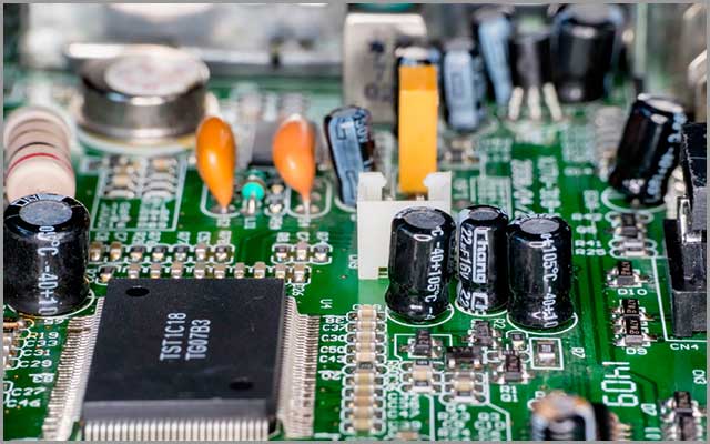 Image 3: Stray Capacitance
4、How to Reduce Stray Capacitance
In many applications, the stray capacitance between multiple signal lines could deplete or impact the design. It is worth mentioning that at lower frequencies, the stray capacitance can often be ignored. However, it could be the main problem in electric circuits at high frequencies. We can control stray capacitances at the layout level.
Stray capacitances often arise due to an electrical coupling generated between a signal line and the other signal line or the substrate and a signal line. It is worth mentioning that it can become essential to lower the stray capacitance of a specific net regarding other signals in many designs.
These are a few of the most effective methods for decreasing stray capacitance:
1. Increasing the spacing between the various nets from the specific set is crucial (stray capacitance is quite important).
2. I am using higher metals for those nets where the stray capacitance is vital.
3. Avoiding excess parallel routing of metals
4. Place another reference signal between networks that require low (where the stray capacitance is not essential). It is called shielding.
This chapter discusses four ways you can reduce. In the next section, we will discuss stray capacitance in transformers.
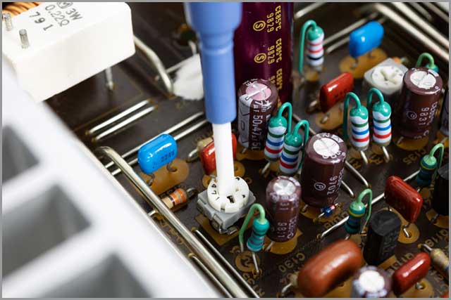 Image 4: capacitances at the layout level
5、Stray Capacitance in Transformer
Transformers are necessary circuit elements like inductors and resistors (Smil, 2017). They are used in almost all electronic systems that operate from AC power. Hence, they're widely used.
Ideal transformers pass voltage to secondary from primary using pure magnetic mutual induction (Han, Chau, and Zhang, 2017). As the primary is inductive, any transient voltage surges are likely suppressed. Also, remember that high-frequency harmonics and noise don't have sufficient energy to induce a voltage magnetically. Ideal transformers, in other words, could be considered low-pass filters.
It is worth mentioning that any two conductors in proximity are bound to form a capacitor.
Adverse effects of Transformer Capacitance
• High voltage spikes of a transient nature may get transferred from a primary transformer to the secondary via capacitive coupling.
Solution
• Use a copper shield between the primary and secondary transformer.
• Use a quality second bobbin transformer.
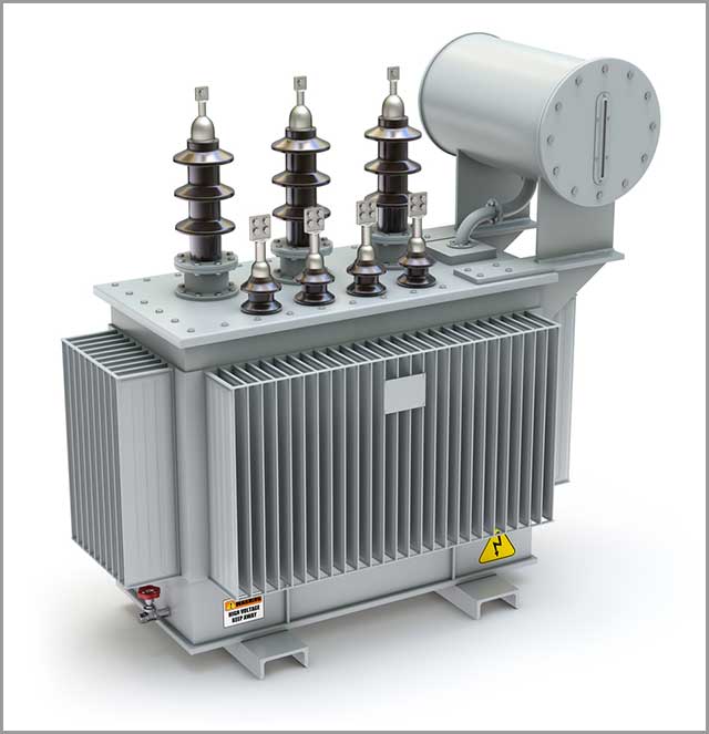 Image 5: Adverse effects of Transformer Capacitance
6、Conclusion
This was a primer on stray capacitance, encapsulating all the information. We hope you like it and will make the most of it.
OurPCB is your reliable source for all types of free information regarding PCB manufacturers. We have what you need whether you are looking for PCB prototyping or need PCB assembly. You can contact us if you are seeking a solution that meets your needs. Our engineers and experts will answer all your questions at their earliest convenience. Our PCB knows how to look after your interests and needs. Could you email us at [email protected]?
Special Offer: Get $100 off your order!
Email [email protected] to get started!