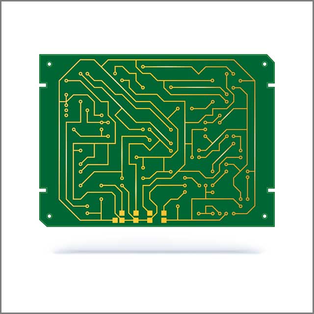
Trace refers to the network of wiring, copper, insulation, and even fuses that make up a printed circuit board when it comes to printed circuit boards.
In nearly all cases, if something is faulty with almost any given electronic device, the chances are excellent that there are inconsistencies involving the PCB trace.
Do you find yourself wasting time and energy trying to fix a circuit board, not knowing what calculations to perform?
Are you looking for a guide that will show you precisely what calculations to do (if measures are even necessary) when detecting trace resistance?
If so, read on. You will find all the information you need right here.
Contents
- Ⅰ. What is PCB Trace?
- Ⅱ. PCB Trace Thickness
- Ⅲ. PCB Trace Resistance-What Is It and How To Use
- 1. Calculation in PCB Trace Resistance
- 2. PCB Trace Resistance Calculator-How do you Calculate Trace Resistance?
- 3. Power Loss and Interference
- 4. Design Optimization
- Ⅳ. PCB Trace Width Calculator – The Ultimate Guide to How to Protect PCBs
- 1. What is a PCB Trace Width Calculator
- 2. PCB Trace Width Calculator Type
- 3. PCB Trace Width Calculator Formula/How is PCB trace width calculated?
- 4. PCB Trace Width Guidelines
- 5. Trace Width Calculator FAQ
- Ⅴ. PCB Trace Repair
- 1. What to know before attempting a repair
- 2. If you do not know your trace resistance and trace width
- 3. When is a repair necessary?
- 4. What to pay attention to when attempting a repair
- Ⅵ. PCB Trace Current
- 1. The power source of a current
- 2. What currents entail
- 3. What to know before calculating a current
- 4. PCB Trace Current Capacity-What Should You Know
- Ⅶ. PCB Trace Width vs. Currents: A table
- Ⅷ. Conclusion:
Ⅰ. What is PCB Trace?
Like a current, trace is an essential part of nearly every circuit board. If it is not detected or calculated correctly, it can take a lot of time and resources to fix. In the worst case, it can cause errors on any device in the system.
Printed circuit boards have many components, and knowing exactly which parts and materials are needed to repair or assemble a printed circuit board is essential. Knowing what kind of formulas and functions to perform can also get overwhelming.
Ⅱ. PCB Trace Thickness
The thickness of a PCB board holds enormous implications for a designer during the design process of a PCB board. Consistency has essential gravity.
If ignoring it, the PCB board might not function or may result in damage or sparks, which might also cause harm to the components connected to the board.
Because single-sided, double-sided, and multi-layered PCB boards exist, the thickness varies with the PCB board type.
For more information, please see the website
https://www.wellpcb.com/pcb-trace-thickness.html.
Ⅲ. PCB Trace Resistance-What Is It and How To Use
PCB trace resistance is a crucial factor that needs to be calculated and analyzed during the design stage. Every material in the universe has resistance alongside other parasitic properties.
Although copper is the most used material in printed circuit boards, it has different compositions and properties. The PCB trace resistance may lead to various design and implementation issues. The issues increase with the increase in the circuit complexity.
1. Calculation in PCB Trace Resistance
Calculating the PCB trace resistance is as simple as using the ohms law with the known parameters.
Most design suits and development environments have integrated PCBs trace resistance calculators, which can estimate the resistance of the final copper trace on the board by providing the required manufacturing profiles.
And the calculator uses a standard formula to calculate the opposition so it will be constant universally.
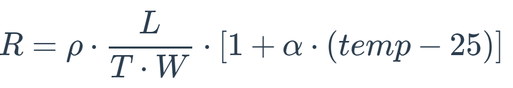
L, W, and T represent the physical area of the trace, i.e., height, width, and length. ΡCB represents the material's resistivity, and α represents the temperature coefficient of the copper. But all of these calculations can only determine a close enough approximate value. The physical cost after production will vary slightly.
2. PCB Trace Resistance Calculator-How do you Calculate Trace Resistance?
Specific formulas printed circuit boards all share in common to operate on a base level. If any part of this formula is wrong, there is no tracking resistance. One widespread mistake people make when detecting PCB trace resistance is that they have no idea how to calculate it.
2.1 Visualizing the Printed Circuit Board
Before revealing and analyzing this formula, we need to know what a conventional circuit board looks like, or at least on the surface. The most common circuit boards possess a thin layer of copper of .009 mm and .38mm in thickness. The most common PCB traces are either 1 oz in weight or .03mm in height.
2.2 The PCB Trace Resistance Equation
Now that we know what a standard circuit board looks like, we can present the formula and put this together. The method to calculate any conductor is as follows:
R = P × area. Each variable is assigned as follows:
R – Resistance.
P – Resistivity of any given material.
Let's use this formula to determine the resistance of pure copper, heated to 25°C.
Pure copper's resistivity rate at this particular temperature is 1.724. Knowing this, we need to multiply it against the area, ranging from 6-10 ohms per centimeter.
Here's another example: Say we have an area of .375mm. If we multiply this by the resistivity, we'll get a resistance of 100 ohms, yielding 20 ohms per centimeter. It is a small value, but it could result in some variance because this formula is imperfect. It is one thing that can affect accuracy in PCB trace measurements.
2.3 Applying the PCB Trace Resistance Equation
Another example of how this can play out is resistance-based current sensing circuits in power systems. If the sense resistor is 1 ohm and you use the same .025mm trace, the system will measure the resistance at 1100 ohms instead of the preferred 1000 ohms.
That is quite a difference, and it can lead to a weaker currency than expected or even necessary.
There do exist ways to work with the trace width that does not involve complicated calculations. These solutions can save time, and you should consider them before performing more complex calculations.
You can regard these options to determine the trace width without needing to calculate the PCB trace width.
The first of these can be done by merely eyeballing the width and increasing or lowering it to see what kind of circuits are connected to it properly. It will do a couple of things.
First, it will increase the copper area, giving you more room for experimentation with different ohm levels. Second, it will reduce the resistance of the copper on the board. It will also allow more testing to determine a proper trace width.
For grid array packages, this is not an option. The option here would be to use a thicker copper layer and place it along with the original circuit board.
It will increase the area and reduce resistance. One thing that should be made aware of is that using a thicker copper layer requires purchasing the proper materials to create a more adhesive copper layer. It will cost some money.
3. Power Loss and Interference
The primary issue in trace resistance is power loss. Small signal PCB will only have a negligible effect on the PCBs trace resistance. But power circuits, on the other hand, will significantly impact even for a slight variation in resistance. Power loss will eventually lead to temperature rise and reduction in conductivity.
In power circuits, uncompensated PCB's trace resistance may fuse if a power surges and burns the trace, leaving permanent damage. While in high-speed digital boards, PCB trace resistance and parasitic capacitance may create oscillation and cause EM interference to the circuitry. Long PCB tracks may also lead to an increase in reissuance.
4. Design Optimization
The most effective way to compensate for the PCB trace resistance is to pay for the resistance by increasing the trace area. Design tools can be configured to lay out traces with sufficient width to avoid such issues.
And power circuits use additional methods other than a complete PCB trace, like solder brides, to reduce the power loss and increase the current capacity. In contrast, sensitive circuits have compensation subcircuits to eliminate the impact of PCB's trace resistance.
And High-speed circuits have matched lines to cancel out the potential interference that may occur due to oscillation.
Special Offer: Get $100 off your order!
Email [email protected] to get started!
Ⅳ. PCB Trace Width Calculator – The Ultimate Guide to How to Protect PCBs
Do you know you have to determine the trace width of PCBs, or they may burn up? Do you know that the trace width is related to the amount of current that it can carry?
You have to know many things, and unless you do everything by the book and the established standards, you risk ending up with a PCB that doesn't work or malfunctions.
That's why we have made this friendly guide to help you determine the trace width of your PCB with a trace width calculator.
We will also reveal the formula so that you can work out the width by yourself!
1. What is a PCB Trace Width Calculator
The width of the traces is a significant consideration when it comes to designing a PCB. PCB designers have to assign an appropriate width to shreds to save them from any damage due to a rise in temperature, which is determined by the current carrying capacity of the board.
The traces on a circuit board are designed to handle a maximum load of current before they fail. When you pass higher amounts of current through a path, it produces heat.
After a time when the current load crosses the maximum limit, the trace will burn out or destroy the laminate of the PCB, resulting in permanent damage.
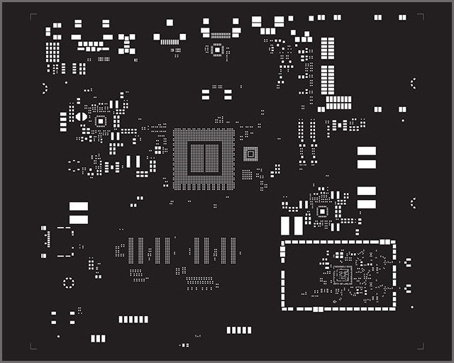
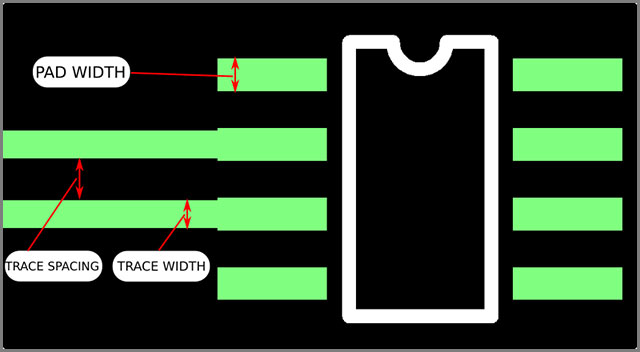
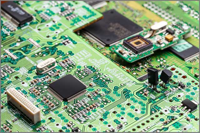
In the picture below, you will see the traces electrically connecting different components and connectors.
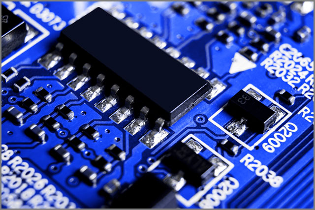
You may think of traces as wires connecting different components with zero resistance, but it is not true. All paths on a PCB come with a specific resistance, which forms an important consideration when selecting the width of the traces.
You have to know the resistance and current carrying capacity to determine which width to use.
The trace width will be determined based on the rise of temperature applicable to a PCB. The increase in temperature denotes the hotness of the trace when you pass current through it compared to when it's left idle.
State it is the difference between the operating and maximum operating temperature.
It sounds like a lot of work and calculations to find out the required width of a trace. However, another easy way you can use- take the help of a trace width calculator.
1.1 Features of Trace Width Calculator
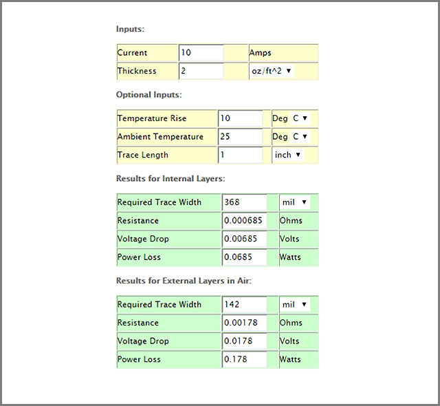
You can use a trace width calculator to determine the trace width based on ampere capacity.
You need to provide your design specifications in the trace width calculators, including the maximum current in amperage that will flow through the trace, the total length of the path, the increase in temperature due to the resistance of the trail, etc.
After you have provided the specifications, the calculator will produce a calculated width for the trace.
The trace width calculator provides you with the minimum width required to match the design specifications you have entered.
The calculated width will allow the current to be passed safely without resulting in damage to the PCB.
To streamline this process and ensure accuracy, you can use an advanced tool like the PCB Trace Width Calculator, which supports real-time input, safety margin adjustments, and multiple industry standards.
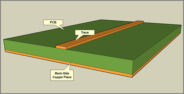
You may find the trace width of the internal layers to be more extensive than external layers as they are prone to produce more heat. The outer layers don't get that much heat due to the convection.
We recommend you use the width of internal traces for the entire PCB for safety reasons.
1.2 Applications of Trace Width Calculators
Trace width calculators are handy when you are designing your PCB. You can use them to determine the minimum width of the traces, safely passing the required amount of current without damaging the PCB.
The trace width calculator will ask for your design parameters to calculate the required width. You may have to input the current to pass in amperes, the thickness of the trace, the rise in temperature, ambient temperature, and the trace length.
The calculator will provide the results for the internal trace layers and external trace layers in the air. You can then apply the values to your PCB design to ensure the proper functionality of the board and the end device or appliance.
It would help determine the minimum trace width for high power signal and power trace applications. However, generally, the traces in a PCB carry calls that use tiny amounts of current. For them, you need to consider other parameters of the PCB to find out the required width.
We have discussed what a trace width calculator and the applications of the tool are. The next chapter will explore the different calculators you can use to calculate your PCB trace width.
1.3 Why calculate PCB trace width?
It may not be sufficient to calculate a general PCB trace or use a simple formula or operation to detect the trace resistance accurately. However, to ensure that the PCB traces turn on correctly, it is necessary to calculate the traces and trace width.
Calculating and significantly increasing the PCB traces' width helps reduce the resistance of any given PCB trace.
1.4 What to know before calculating trace width
Calculating the trace width is much more complicated than calculating any given conductor. There are many things you must know before calculating the PCB trace width.
Among the inputs, You need to know the maximum current that the circuit can work on, i.e., the unit of the measurement trace, the trace thickness, how hot the evidence temperature can get, and the ambient temperature of the trail. It will determine the input ranges of the width.
You will get output figures when you plug those numbers into this calculator. These numbers will tell you precisely what the trace width is.
These figures of trace width include the trace width (measured in amps), the trace temperature (measured in Celsius), resistance (measured in ohms), the voltage drop (measured in volts), and the power dissipation (measured in watts).
All of the input information should be viewed on the physical printed circuit board or on the datasheet of the printed circuit board itself. There should be no guesswork here; any given circuit board should have this information on the bright display.
If you do not put in the exact numbers and measurements you see, the calculator linked above will not allow you to make a calculation. Because printed circuit boards are tiny, you will likely need a magnifying glass to take down the input information.
1.5 Figures to remember
After getting all this information and having the output numbers, take those down and keep them to the side. You now have measurements for both the PCB trace as well as the PCB trace width.
You also know that there are methods of testing individual components of PCB trace to see if there is a width range. Armed with this information, you can now begin repairing your PCB trace.
2. PCB Trace Width Calculator Type
All the calculators that calculate the trace width base their calculations on industry standards. The most common standards in use in commercial and industrial applications take the IPC 2221 and IPC 2152.
Both standards have been developed by the Association of Connecting Electronics Industries, a trade association that sets standards for the manufacturing and assembly of electronic equipment.
Let's find out more about these calculators.
2.1 IPC 2221 Calculator
The IPC 2221 comes from an old standard used previously called IPC-D-275. It was developed in 1954 based on graphs and measurements.
IPC 2221 calculator uses a single graph and an equation for determining the track current denoted by 1. The equation is as follows-
I=kΔTbAc
Where k has a value of 0.048 for the visible traces and 0.024 for the internal tracks, ΔT represents the rise or change in temperature measured in Celsius. B has a value of 0.44, whereas A means the cross-sectional area expressed in mils2. C has a value of 0.725.
You have to remember that you can use only a range of values in IPC 2221 calculators to get accurate results for trace width. The amount of current is 0-35 ampere, the width of copper is 0.5-3oz, the track width is 0-10.16mm, and the temperature rise is between 10 degrees Celsius to 100 degrees Celsius. If you use values outside of the defined range, the results may be erroneous.
The calculator considers the track length adequately long, and the end connectors or components do not affect heat dissipation. For this reason, the calculator may not be able to calculate the parameters for thermal-relief type connections that use a copper pour for a visa.
The calculator also assumes you are not using any via in the track length.
The current to be passed is taken as constant or DC. However, you have the liberty to use the RMS value in case of a pulsed current where the pulses are frequent enough.
You have to keep in mind that the temperature of the PCB should always be within the relative thermal index (RTI) of the material you are using.
You will find the definition in UL746B as the temperature, which allows the retention of 50% of the material properties after 100,000 hours.
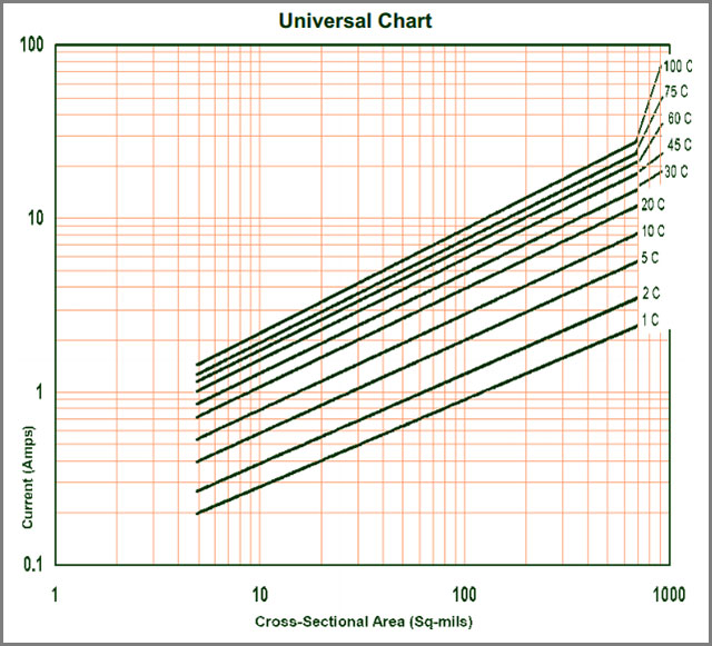
2.2 Calculator IPC 2152
The IPC 2152 calculators base their calculation on a much newer standard, the IPC 2152. It is a more accurate way of determining the maximum trace current capacity through an increased technical approach.
The IPC 2152 calculators don't use a simple equation like IPC 2221 calculators; they must first use a Universal Chart to determine the unadjusted cross-sectional area.
Then the calculator uses a variety of parameters to derive a series of coefficients or modifiers.
The parameters used include the thickness of the PCB, the thermal conductivity of the board, the thickness of the current passing trace, the distance between existing passing tracks and the copper plane, and so on.
The calculator will determine the adjusted cross-sectional area by multiplying the coefficients with the unadjusted cross-sectional area. Then you will be able to access the required width from the calculator.
2.3 IPC 2221 Vs. IPC 2152
The IPC 2221 was developed many years back and did not provide a full-proof method of calculating the trace width of PCBs. The standard did not consider many parameters required to measure the trace width correctly.
For example, the IPC 2221 doesn't consider the board's thickness and material. After several studies and experiments, the IPC 2152 was released in 2009, making it more accurate to calculate the current capacity and trace widths.
IPC 2152 considers several parameters, such as internal vs. external traces, the location of heat-sinking planes, the thickness of the board, and others, to provide a more accurate result. You can also use it for multilayer PCBs at IPC 2221; there was no technology to create multilayer boards.
You learned about the different types of trace width calculators based on standards IPC 2221 and IPC 2152. Now we will take a look at the trace width calculator formula.
3. PCB Trace Width Calculator Formula/How is PCB trace width calculated?
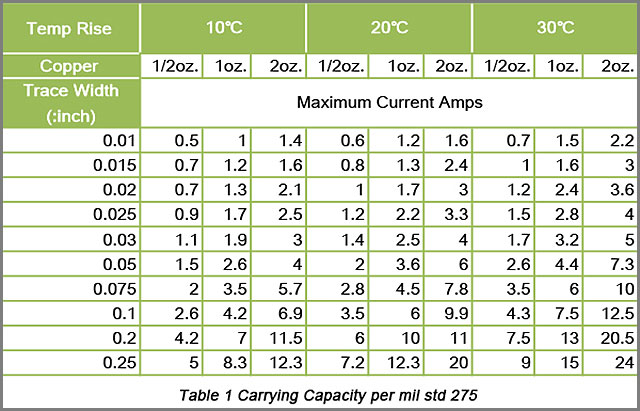
3.1 PCB Trace Width Table
The PCB trace width table can help you determine the trace width of your PCB. It also gives you an idea about the current carrying capacity and the impact of the temperature rise.
Keep the trace width table handy to be used for your applications. The table is given below for your convenience-
3.2 PCB Trace Width and Spacing
Using a trace width calculator, you know how to derive the trace width. You will need to rope in many considerations, such as.
- The current carrying capacity of the trace
- The pitch and size of the pads of the components the trace will be connecting.
- The gap between traces
Besides the trace width, it is also essential to consider the spacing between the traces. It will prevent short circuits and allow maximum space between atoms for proper functioning.
PCBs are generally small as it relates to the cost of production. However, if the board is too small, you may find it difficult to route the traces and maintain proper spacing between them. You can keep a 6 to 30 miles spacing, which is enough for most signal trace widths.
3.3 PCB Trace Width Formula
You can find the trace width of your PCB using the formula for calculating the allowable current passing through a trace, as defined under IPC 2221. The procedure is as follows
I=k*ΔT^0.44*A^0.725
I in the equation stands for current and is taken as a constant. ΔT refers to the change in temperature, and A represents the cross-sectional area of the trace.
You can now rearrange the formula to derive the trace width by finding out the cross-sectional area for the chosen currency to pass through safely.
Area[mils^2] = (Current[Amps]/(k*(Temp_Rise[deg. C])^ 0.44))^(1/0.725)
You have to consider then the thickness of the trace to find out the desired width.
Width[mils] = Area[mils^2]/(Thickness[oz]*1.378[mils/oz])
The formula can be used for 0 to 35 amperes of current, allowing the temperature to rise from 10 degrees Celsius to 100 degrees Celsius. It accommodates 400 mils trace width while you can use 0.5 to 3 ounces of copper values.
The above formula is used as an industry standard and is assumed to be accurate. It may not be appropriate for all designs, and the website is not responsible for any damage resulting from using the formula.
In the next chapter, we will tell you the general guideline to follow while determining the trace width for your PCB.
4. PCB Trace Width Guidelines
4.1 PCB Trace Width Rule of Thumb
The trace width of your PCB will depend on the design specifications and the amount of current you want to pass through the tracks. There is a general rule of thumb that you can follow for most of the applications.
The minimum trace route width to apply is 1.0 mm/A. It is applicable for 1.0 oz/ft2 of copper thickness, commonly used for various PCBs.
We have almost come to the end of our guide. We will wrap things up with a quick FAQ on trace width calculators.
5. Trace Width Calculator FAQ
5.1 Do you have a limit on the amount of current this calculator uses to find trace width?
A: You can only use currents of up to 35 amperes, a temperature rise from 10 degrees to 100 degrees Celsius, copper from 0.5 to 3 ounces per square foot, and trace width up to 400 mils. These are the limits based on the IPC 2221 standards. Using any value outside this range can lead to inaccurate results.
5.2 Generally, we think about the width of the traces in the internal layers.
It would be lesser than the visible traces as they can damage the board when heated significantly. However, the calculator shows the opposite results. What is the reason?
A: The traces in the external layers can transfer heat more efficiently as they are in contact with the air. The heat dissipated through convection, and the atoms do not get heated up too much. However, the traces on the internal layers don't conduct heat as efficiently as the external layers.
As the calculator is meant to prevent an undue temperature rise, it increases the width of the internal traces as they store more heat. When using a potted assembly or a circuit in a vacuum, you should use the width of the inner layers as the external layers cannot transfer heat.
A: The temperature rise denotes the difference between the operating temperature of the PCB and the maximum operating temperature of the board material. The copper traces produce heat as you pass more current through them.
While designing a PCB, you can account for the added warmth and choose an appropriate width according to it. 5.3 What does the calculator indicate by a rise in temperature?
You can go for a temperature increase of 10 degrees Celsius, as it is safe for most applications.
Ⅴ. PCB Trace Repair
1. What to know before attempting a repair
Before attempting any form of PCB trace repair, you must know the exact measurements of the PCB trace resistance as well as your PCB trace width.
Because you are now working with physical objects and not measurements, you will save much time, money, and trips to wherever you buy your equipment if you know your measurements.
2. If you do not know your trace resistance and trace width
measurements or have an idea, and you perform repairs at the risk of your own time and money. If you feel like you can take an educated guess at the PCB trace resistance and PCB trace width of your selected electronic device, it could save you time performing guesswork with the wires you will measure and connect. Feel free to do that.
3. When is a repair necessary?
PCB trace repair is needed when the following things have happened to the device that it provides a current to:
- The method still works, but there are visual issues with the display.
- The battery of the invention is fresh and wholly charged, but the device does not power on
- If the machine produces sound, such as a speaker, music is distorted (the speaker has not met with any physical impact)
If any of those things affect the PCB-powered device, the PCB trace likely needs to be repaired.
Printed circuit boards connect to copper, fuses, wiring, and insulation. You must know many things about how the wiring and insulation intertwine when it comes to these things. This brief guide can provide some information and can reduce complications.
4. What to pay attention to when attempting a repair
One thing that you should especially notice is the maximum current that the board can operate.
If too much power is from the current provided, you will experience a short circuit and risk losing the circuit board when testing out the repair. Err on the side connecting a wire with a lower current for the circuit board.
Again, this is why it is essential to know the trace resistance and width of the printed circuit board. Understanding the PCB trace current is the next step in handling a faulty printed circuit board.

Ⅵ. PCB Trace Current
1. The power source of a current
Printed circuit boards use a direct current as a power source. It is much different from a PCB trace, which provides how the wiring and other conductors interact to provide this current. It means that there is only one flow of a present that travels through the wiring and copper of the circuit board, where the electrons travel straight to the battery, which then powers any given device.
PCB trace currents are critical to recognize as they are just as necessary in constructing a printed circuit board as the trace resistance and width.
The trace and trace width of any given printed circuit board could be measured correctly, but if there is only one error in the PCB trace current, the device is not working correctly and requires extensive repairs.
And even more so, if there is no current in any given printed circuit board, there is no power.
2. What currents entail
Any given electrical currents utilize conductors and insulators in their calculations. In printed circuit boards, most use copper as a conductor and rubber as an insulator.
The relation between these two is balance: If proper insulation does not protect a conductor, too much power will be generated, and a short circuit may occur.
Suppose the insulator of a printed circuit board is too large. In that case, the reverse will happen: Not enough power will be generated, leading to the substandard performance of any given electronic device that uses a printed circuit board.
Electrical charges and currents in a printed circuit board are usually measured in amps. Most of the time, there will be a specific limit as to how much power any given printed circuit board can allow before there is a short circuit. It is something that deserves close attention.
3. What to know before calculating a current
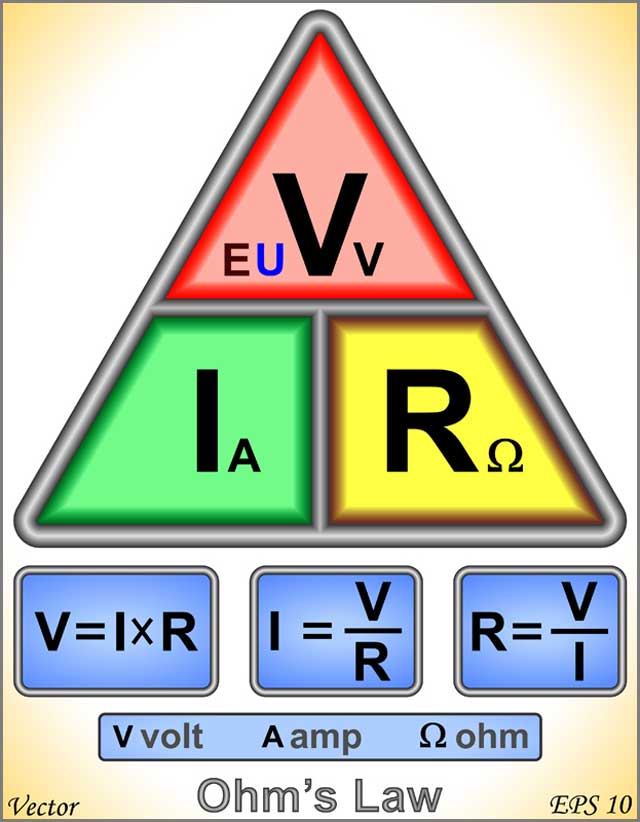
When calculating the charge or current, it is necessary to establish the relationship between amps, volts (measured voltage), and ohms (determined resistance).
This relationship is depicted in a formula derived from Ohm's law, which states that energy is equal to the product of current and resistance.
From Ohm's law, it is possible to create a simple formula from this inverse. Dividing voltage into resistance will determine what the proper current of a printed circuit board should be.
4. PCB Trace Current Capacity-What Should You Know
In the early days, we used the printed circuit boards to link the low power circuitry. And high-power circuitry was made using point-to-point jumper wiring to compensate for the high current carrying needs.
As the boards evolved, the copper layer was optimized by spreading. It is over ample space and high-resolution isolation from low-power rails.
4.1 PCB Trace Current Capacity/How much current can a PCB trace handle?
PCB Trace Current Capacity cannot surpass the right old think copper wiring. But it can reduce space consumption exponentially. Various design aspects and material properties determine the PCB trace current capacity.
For example, the most common use of 1oz copper offers approximately 500mΩ per square inch. So, you can increase the capacity by increasing the effects on the current path.
PCB trace current capacity is calculated during the PCB design stage. And the traces are laid out accordingly.
Most PCB design suits have an integrated trace width calculator or the equivalent option to determine the trace thickness according to current needs. The copper thickness of the board is designed.
However, you have to do a more advanced simulation to study the effect of high currents on other circuitry and heat dissipation factors. Because, unlike the thicker copper wire, a small surge can fuse the trace resulting in total damage to the board.
PCBs trace current capacity calculations must also include integrity and power loss. To predict the maximum limit and peak operating temperature.
The PCBs trace current capacity calculation has to be optimized to prevent the surge in the production cost of the PCB.
Ⅶ. PCB Trace Width vs. Currents: A table
The following table will put everything together by comparing a PCB trace width and a PCB current. There are similarities and there are differences in these figures.
Knowing the difference between the PCB trace width and the currents that flow within a printed circuit board will give you a much easier time should you decide to repair and troubleshoot any given printed circuit board.
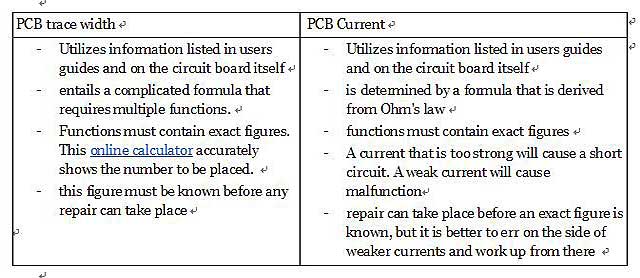
The best thing to do before repairing a printed circuit board is to figure out the trace width and the current and then find the proper fuses, wires, and copper plates that match everything up correctly. It's easier to take action when you know precisely the trace width and current of the printed circuit board.
Ⅷ. Conclusion:
I hope the above information about PCB Trace is helpful to you. PCBs are the backbone of different electronic components and appliances. There are several considerations to keep in mind when you design a PCB.
Special Offer: Get $100 off your order!
Email [email protected] to get started!